 Vedran
Introduction
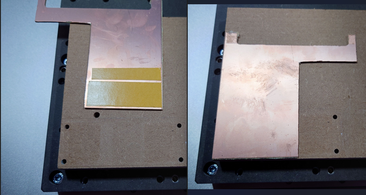
I've always been intrigued by the possibility of making circuit boards at home. So when I got a CNC machine, one of the first things I wanted to try was fabricating custom-made circuit boards. I focused on creating a reliable process that can be easily followed and is almost guaranteed to produce same result over and over again.
Despite it being a DIY process, I was still interested in creating boards that are somewhat comparable to commercial ones, which meant having a soldermask, and (to some extent) silk screen. At the same time, I was not under the illusion that it will ever match what you can get from many online PCB fabrication places, but it's sufficient for most hobby applications.
This process shown here covers producing a double sided circuit board using Makera's Carvera CNC machine. It's desktop-size machine with work area of 36 * 24 cm, 200W spindle, accuracy in the range of <0.01mm and integrated 2.5W laser module. However, to some extent, this process can likely be applied to just about any CNC machine.
The process covers:
- Drawing and exporting a PCB in KiCAD
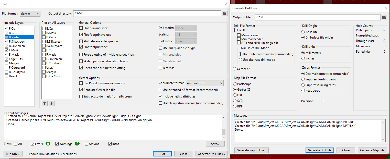
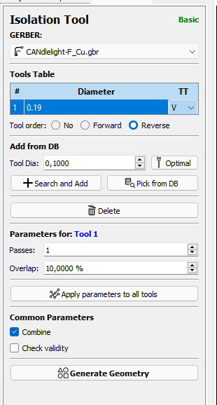
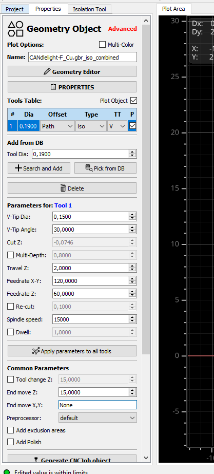
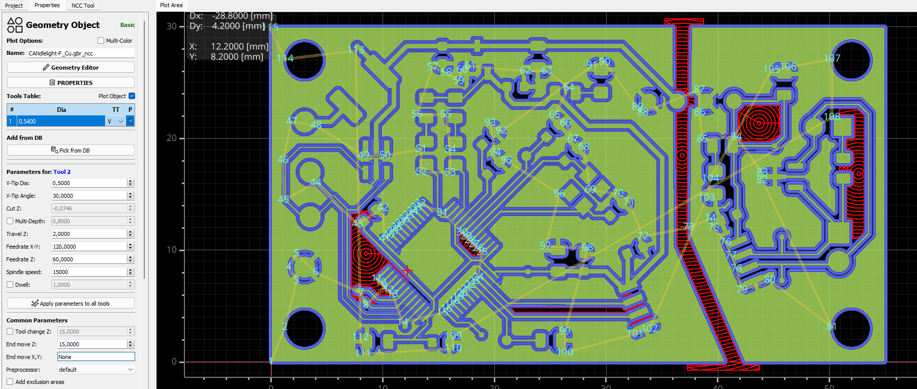
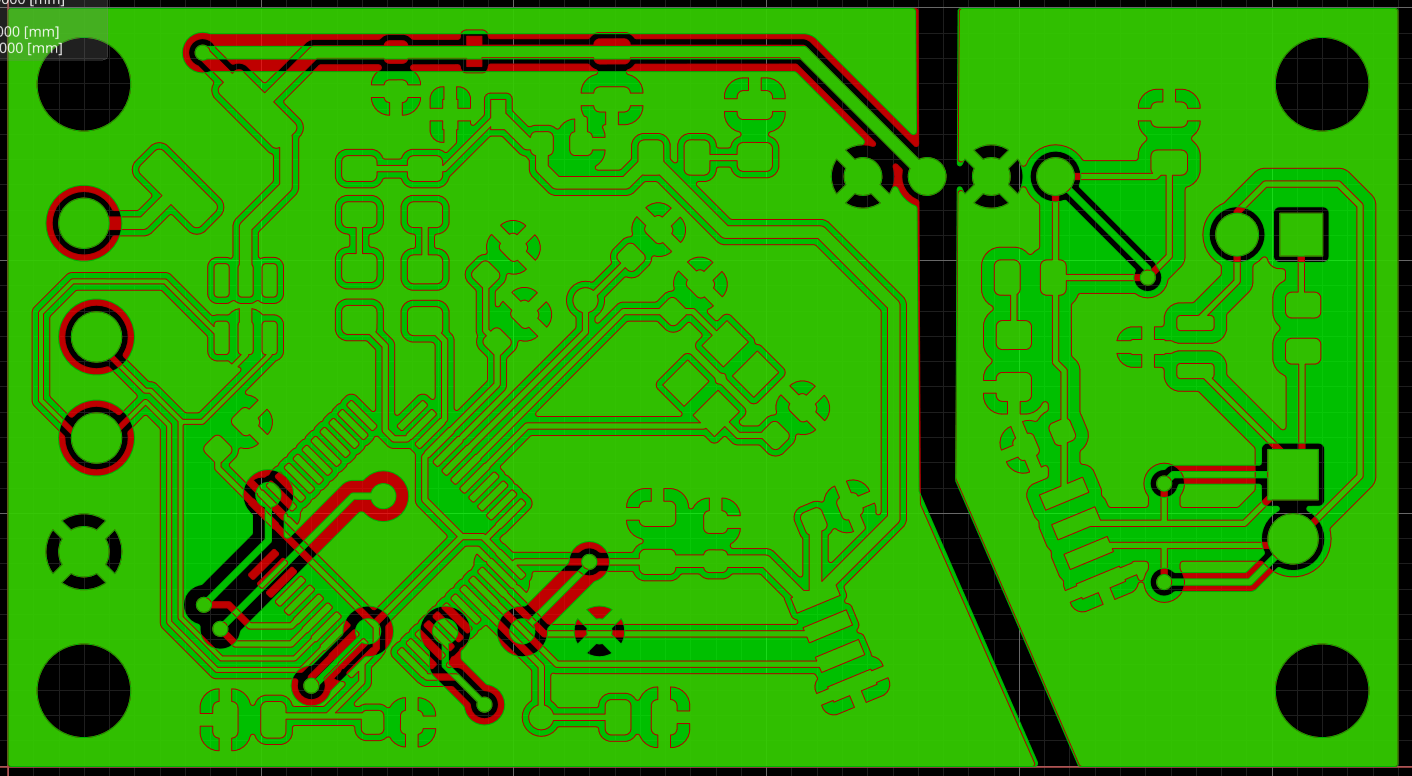
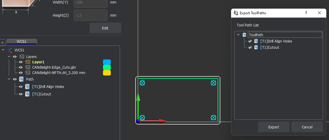
- Creating routing job using FlatCAM
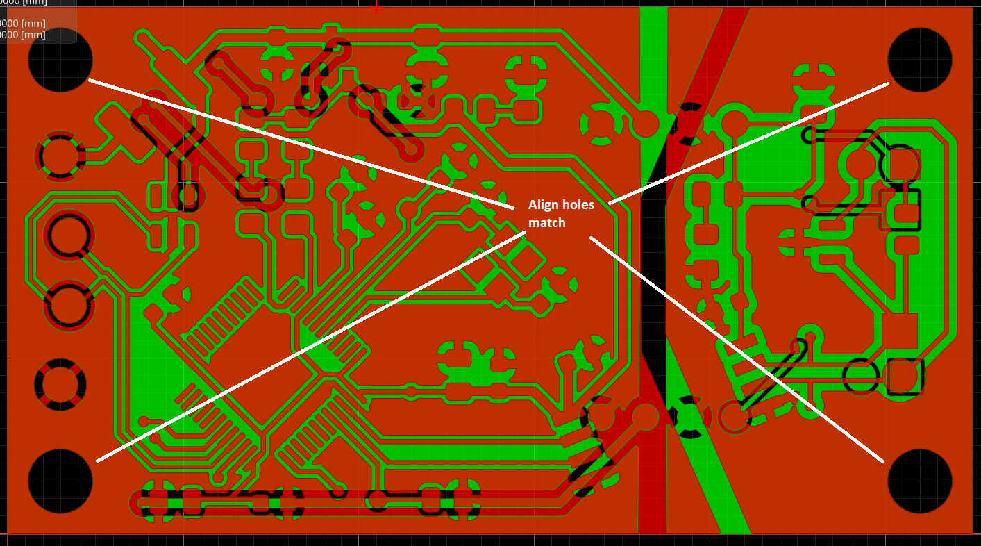
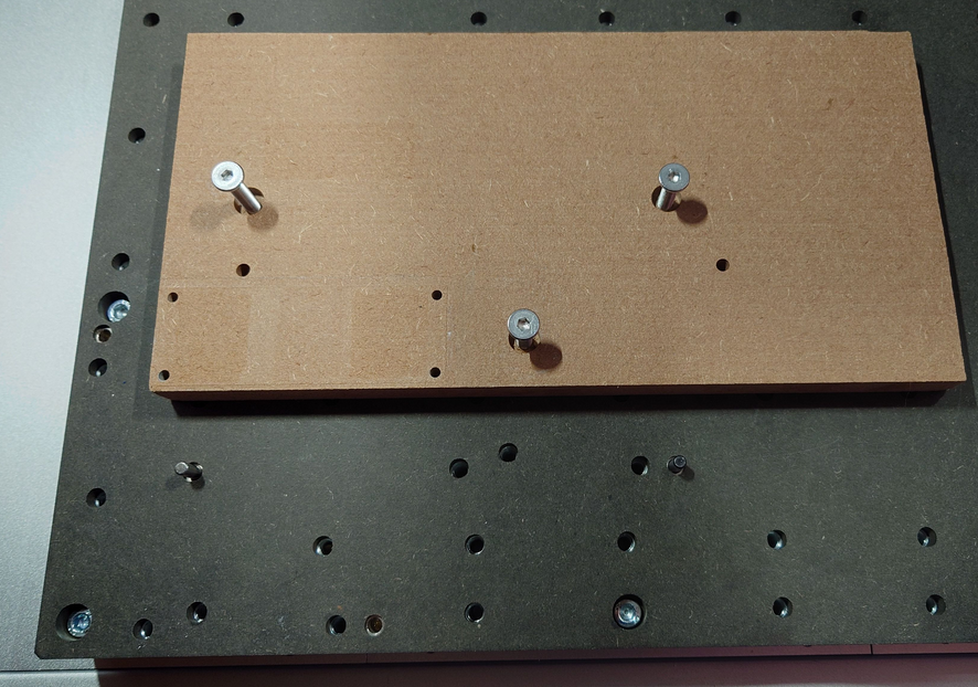
- Preparing a board cutout and align holes using MakeraCAM
- Routing
- Applying solder mask
- Removing solder mask from pads
- Flipping and aligning the board
- Applying silk screen
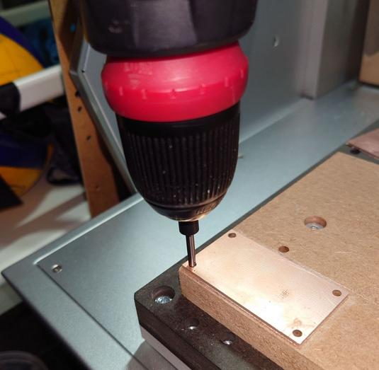
- Drilling holes for through-hole components
- Creating stencil
Finally, I'd like to point out that there's not a lot of novelty in this process, it's a collection of different techniques made with inspiration from others seen online. There will be credits through the guide to different sources.
Limitations
So far, this process has been reliably test out on components as detailed as LQFP48/64 package. This means package size of 10x10mm and pads of ~1.2x0.25mm, spaced 0.5mm apart.
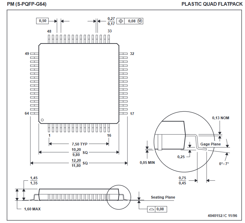
(source: https://www.ti.com/lit/ds/spms376e/spms376e.pdf, p.1404)
This was also used as an inspiration for design rules when making a PCB. Namely, minimum trace size of 0.2mm and clearance of 0.2mm.
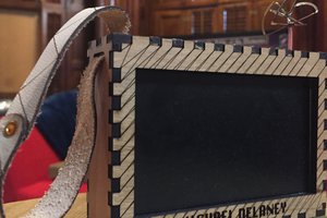
Here's few of the examples made with this process:
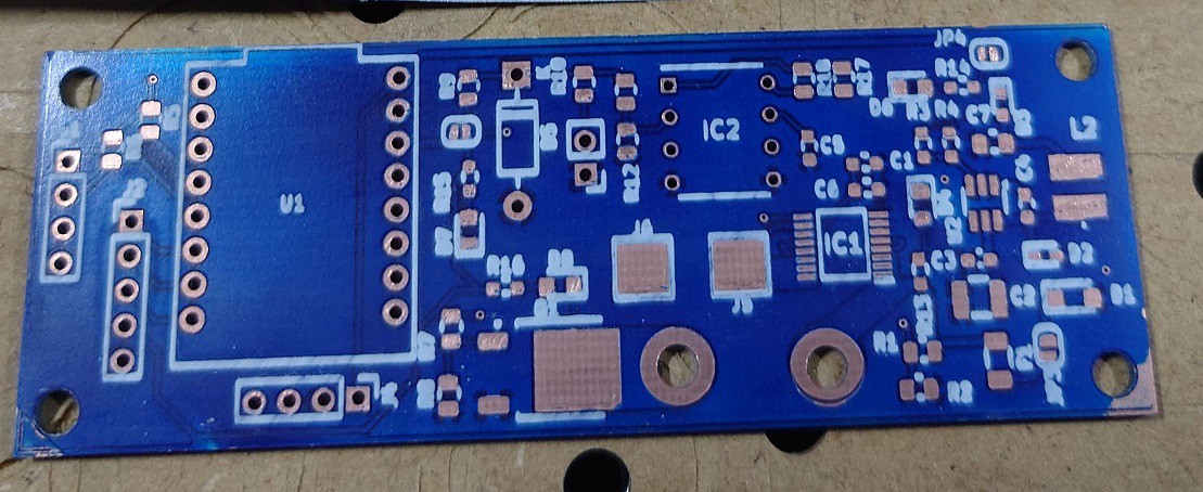
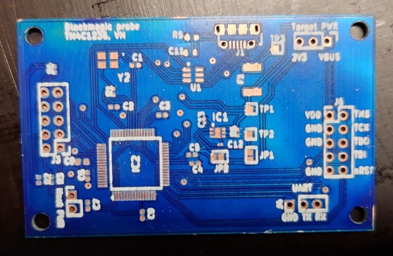
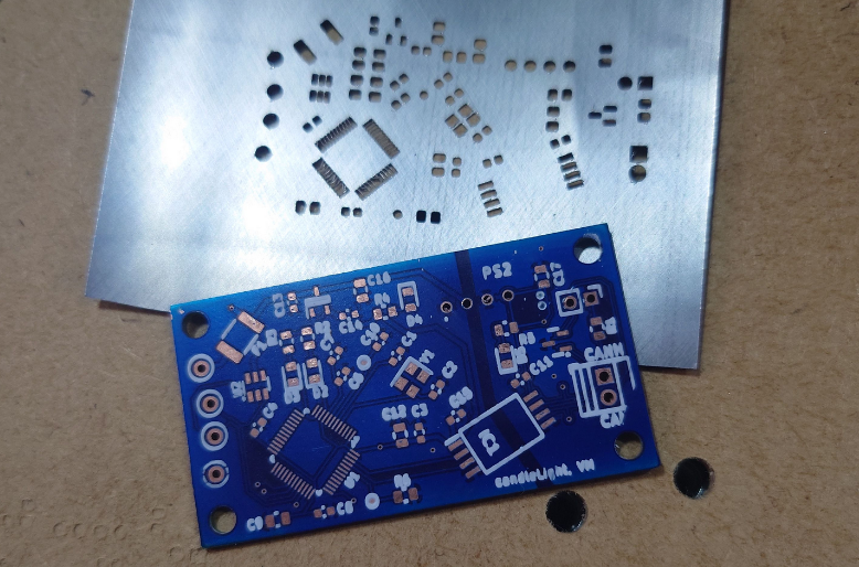
This rest of this guide is going to follow a whole new board from scratch to the final result, shown in the last picture. See "Build instructions" section below.
Future improvements
Currently, my biggest problems with this process is the lack of plated holes to connect top and bottom copper layers, which requires them to be manually connected by soldering a component on both sides. If a component blocks access to pads on top copper, other shenanigans need to be employed like connecting the pads with a thin wire through the hole, before soldering the component, or stitching the top and bottom signal with a nearby via. In the future, I would like to incorporate rivets mentioned in this guide into this process to fix this problem.
Second thing that bothers me is the resolution of the silk-screen. It's rather chunky and I would like it to be thinner. I already tried adjusting the focus of a laser, but I'm not convinced that's the problem. Namely, just burning the same text into wood can be done at a much better resolution. My future improvements will also focus on that.


 Michael Delaney
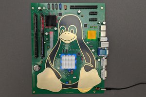
 Ian Dunn
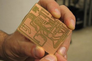
 PCB designer
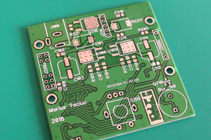
 Marius Taciuc
great work! its hard to find references to flatCAM with carvera , especially with the project file included!!