Place symmetrical align holes, for example a hole in every corner, exactly 3mm from the edge
Place board "Grid origin" and "Drill/Place File origin" points in the bottom left corner of the board
Take special care of through hole components! This PCB doesn't have plated holes and so the component needs to be soldered from both sides in order to link top and bottom layer. KiCAD will by default link signals or ground planes using a through hole component, in the same way it does with a via. However, some components might cover the top side, making it unavailable for soldering.
For through-hole component that cover the soldering point on the top layer, it might be a good idea to route a "backup" track on the back layer, just in case it's not possible to solder them from the top, or only route on the back layer where you're sure to get good contact.
Finally, before exporting, make sure to run design rule check to ensure no silly mistakes spoil the design later (e.g. silk screen placed on top of a copper pad).
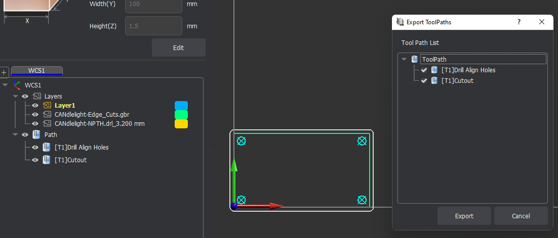
Export
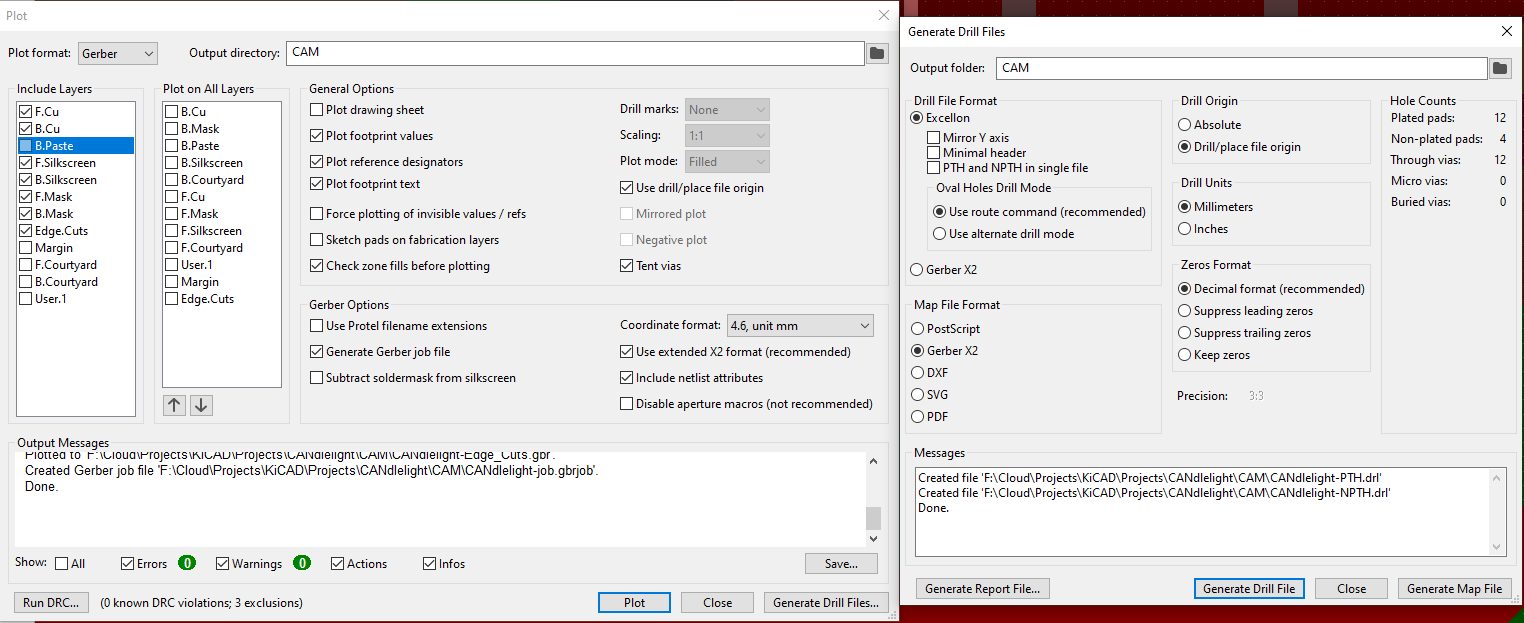
To export the files, navigate in KiCAD to Files -> Fabrication output -> Gerbers (.gbr) ...
Set output directory, e.g. "CAM"
Include layers: all copper, silk, mask and edge cuts
Under "General options", select "Use drill/place file origin"
Before export, it's a good idea to run design-rule check. This will provide feedback on any unconnected tracks, overlapping silkscreen etc that should be fixed
Finally, press "Plot" to export the files
Then, press "Generate Drill Files" to export drill patters and sizes
In the new window, make sure "Drill File Format" is "Excellon" and "Drill origin" is "Drill/place file origin"
Finally, press "Generate Drill File"
Close both dialogs
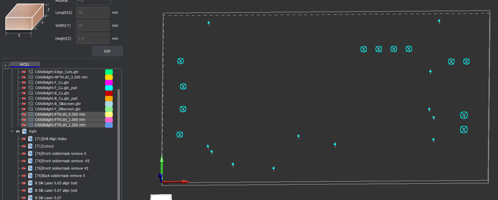
2
FlatCAM
Isolation Routing
To process exported files into a CNC job, we'll use FlatCAM.
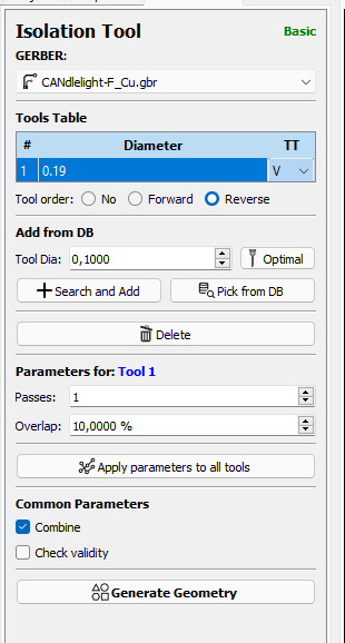
Start by importing F.CU layer
Double-click the layer and and select "Isolation Routing"
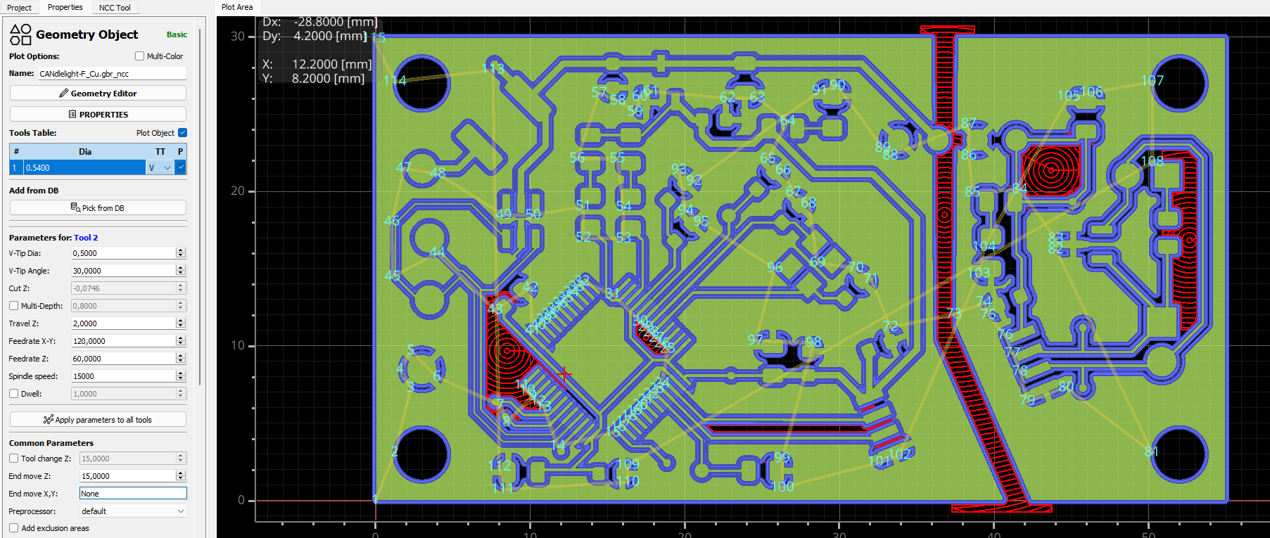
In the tools table, we'll set tool diameter to 0.19mm. This has to be lower than the "Minimum track clearance" setting in KiCAD to ensure correct routing. As a side note, I'm using 0.2mm V-bit for isolation routing. So the correct setting here would be 0.24mm instead. So in reality, all the pads and tracks will be 0.05mm undersized. I have tried this step with bit diameter as low as 0.1536mm for a 0.2mm bit, and the results were still satisfying.
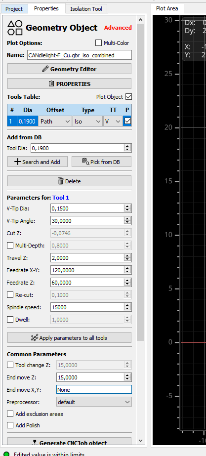
To generate the CNC object from geometry, set V-Tip diameter 0.15mm for cutting depth of -0.0746mm. Spindle speed 15'000 rpm.
Settings
Copper clearing
Usually, it's enough to just do isolation routing, but sometimes, there's the need for clearing copper areas. FlatCAM has NCC feature for that.
This can be used to generate geometry and a following CNC job. In this example, I'm using a 0.5mm V-bit for clearing larger areas of copper.
Back Isolation Routing
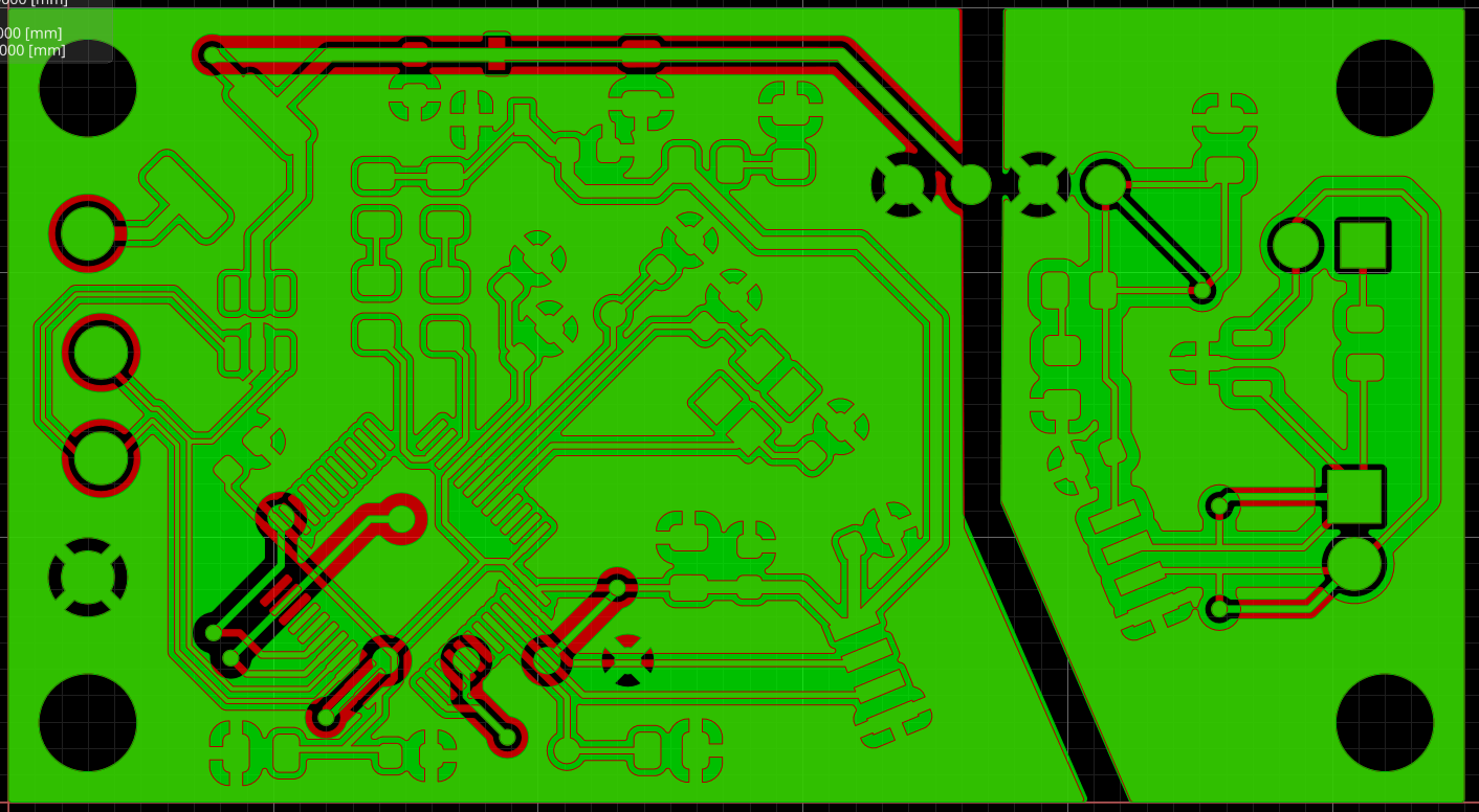
Next, import back copper layer. Before generating geometry and job, the imported gerber object needs to be flipped in either X or Y axis. I prefer flip around Y axis.
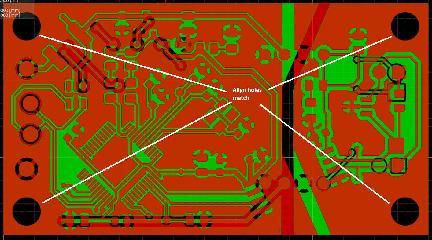
To do so, double-click imported gerber object, and press "Transformations" button from the side menu. From there, press "Flip on Y" from the "Mirror (Flip)" side menu. Using the 4 align/mount holes, confirm alignment between the front and back copper layer.
Before back layer Y flip
After back layer Y flip
From here on, repeat the isolation routing and copper clearing steps in the same way as for the top layer.
Export cnc jobs
The above will result in 2 to 4 ".nc" files (isolation and copper clearing per copper layer), CNC job to run on the machine. To make this work with carvera's tool changer, a small tweak in ".nc" files is needed as outlined in the video here.
3
Fixture + Cutout
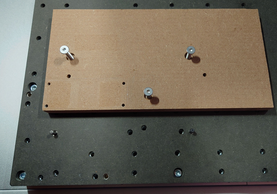
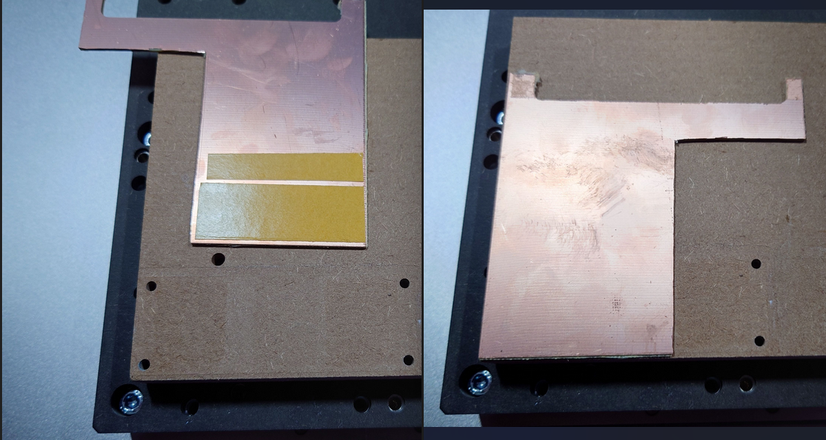
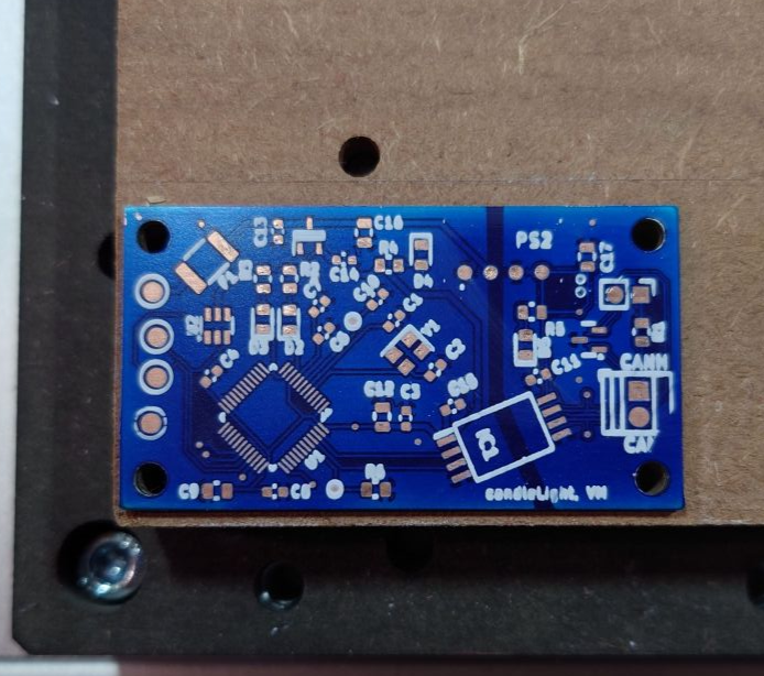
To work with PCBs, I create a fixture that aligns on carvera bed using pins, and is fastened with 3 screws (file attached here). This fixture has also been milled so that its top face is flat. On the fixture, the bottom-left hole is placed at coordinates (5,5) from the anchor point 1, and it's where I'll have my bottom-left align hole for the PCB.
I always start a PCB project by adding a raw PCB to the fixture, drilling the align holes and cutting the board to the correct size. To create CNC job for that part, I use MakerCAM. Import EdgeCuts and NPTH layers from KiCAD export into MakeraCAM. Select the align holes, and create "Vector Drilling" task for them, end depth of 10mm (to go through the board and create align holes in the fixture for later). Secondly, select the edge cut vector, and create "Vector Contour" job with end depth of 1.6mm. Both the holes and the cutout are made with 1/8" x 12mm single flute bit, in my case set as tool #1. Export both toolpaths together in a joint file, and import to Carvera controller.
When running the job, set the offset from anchor point in controller such that the bottom left mount hole on the PCB aligns with the bottom left hole in the fixture. I always place that hole on PCB at coordinates (3,3) from origin and since the align hole on fixture is at (5,5), it gives an offset of (2,2).
The PCB is secured to the fixture with double sided tape.
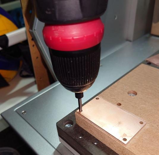
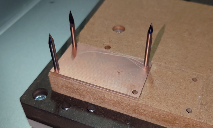
Once the job is completed, clean up the dust chips from the board and leave it stuck to the fixture. Use the newly made holes and a 1/8" bit to test the alignment on at least 3 holes at the time. The holes might be a bit tight at this point, you can carefully widen them with a 45 deg chamfer bit in a hand drill.
4
Front Copper Routing
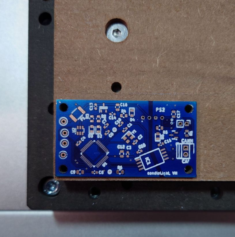
After ensuring the alignment, we can do isolation routing on top copper layer. Load isolation routing job from Flatcam, ensure you have the tools correctly setup (in my case, tool 2 is 0.2mm V-bit for isolation and tool 3 is 0.5mm V-bit for clearing). Since the holes were previously made in size 1/8", old/damaged tools can be used as alignment pins. After confirming the alignment, remove the alignment pins from the holes.
In carvera controller, load the front copper isolation routing .nc file, ensure correct offset from anchor point (same as in previous step) and set the job to run auto leveling on 5x5 points before starting.
After the isolation routing has completed, load and run a copper clearing job for front side (if necessary) without restarting the machine. Remember to disable both auto leveling and z-probing - the goal is to reuse existing height map from isolation routing.
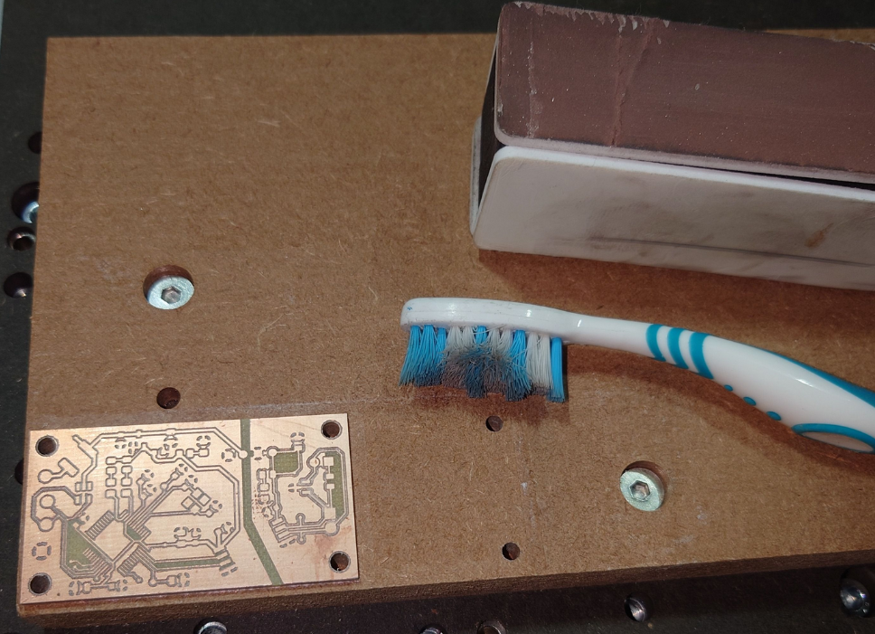
The top copper layer is now done. It should be sanded with a very fine sand paper, and I give it a good brushing with a toothbursh, to make sure no copper is left over within the milled lines to cause short circuit between adjacent tracks.
Finally, wipe the board using alcohol before proceeding to applying soldermask.
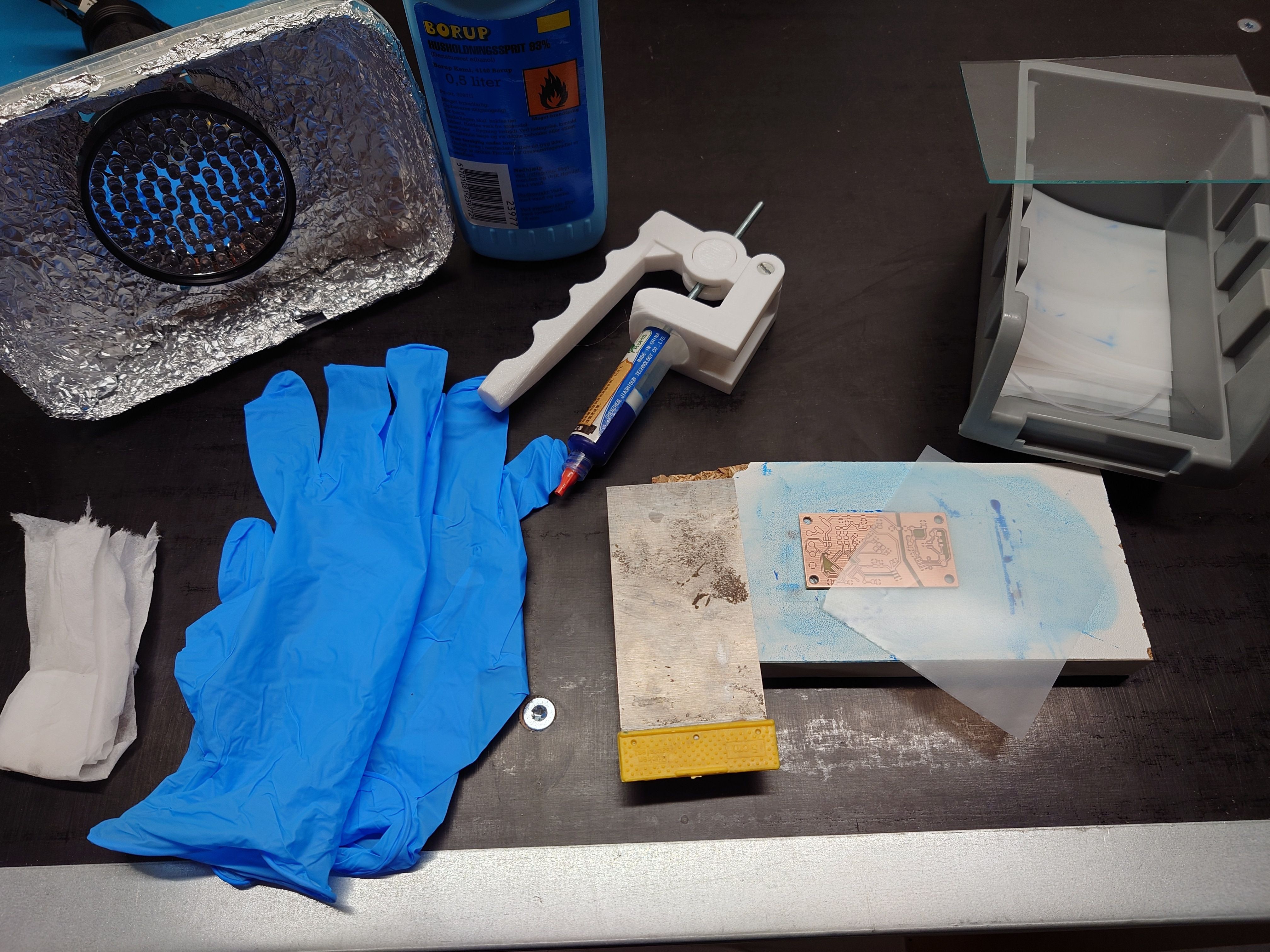
To apply the soldermaks, we need a couple of things
Gloves, to avoid contact with the resin
Alcohol and some paper, to wipe the copper surface before applying the soldermask
More paper, to clean the tools from soldermask resin
UV curable soldermaks resin
Spatula, to initially spread the resin evenly
Plastic sheet, to put on the resin on PCB to separate it from glass
Glass, to press on the resin to help it spread evenly
UV lamp (or sunlight), to cure the resin
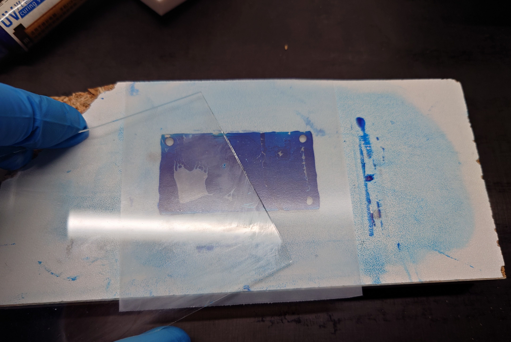
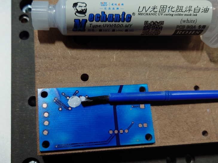
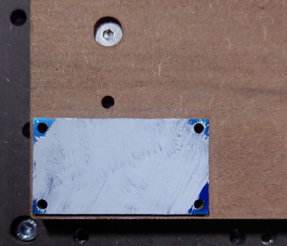
First, secure the PCB onto a working surface and squeeze some solder mask resin onto the PCB.
Then, use a spatula to spread it around somewhat evenly.
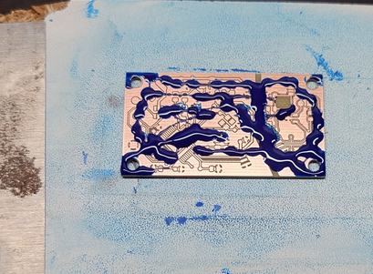
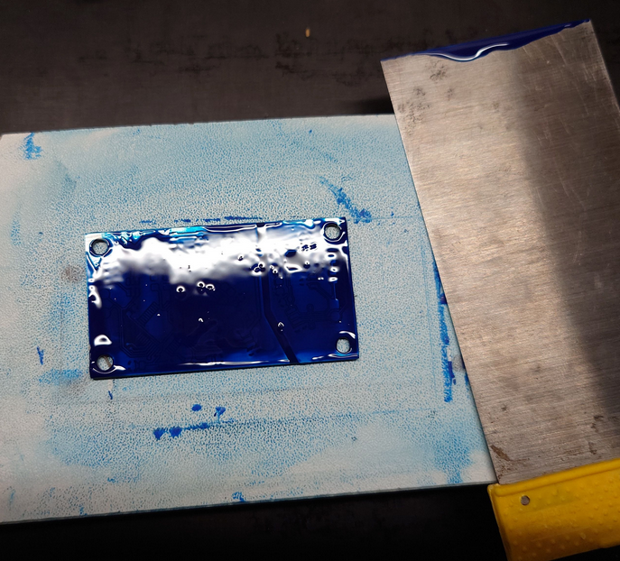
Then cover the board with a thin, transparent plastic sheet. These are something I had laying around, perhaps a transparent foil for laser printing could work here. Use a glass pane (from e.g. a picture frame) to further spread the resin around and remove potential air bubbles under the plastic sheet.
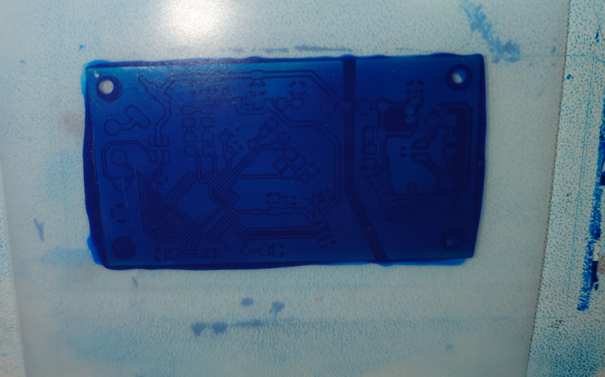
Final result should look something like this. Even spread shown by even color of the resin, thin enough to still see the routing underneath, but thick enough that no copper color comes through. This part takes a bit of getting used to, but if you're not satisfies with the outcome, it's possible to wipe the resin from the PCB with alcohol and try again.
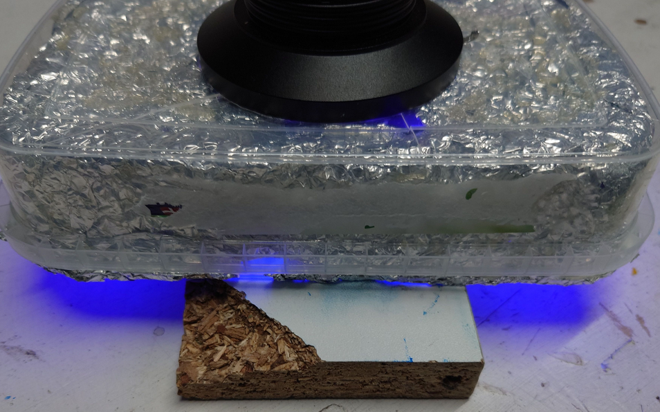
The board can now go under UV light for curing. Cure for 3 minutes with the plastic sheet on, then gently peel it off, and cure for additional 10 minutes.
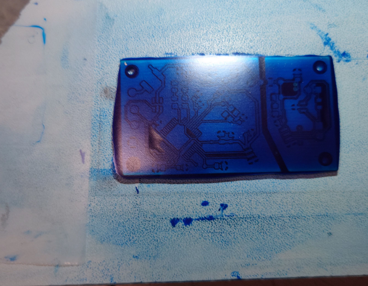
The resin is cured and the board can be cleaned up.
This includes wiping it with alcohol to remove resin residue from the sides, and cleaning up the align holes. Use a hobby knife to remove cured resin poking from the sides of the board.
Avoid using power tools (like a hand drill) to clean the semi-cured residue from the align holes as that might ruin the holes and consequently the alignment. Preferably use a small drill bit (e.g. 2mm) and drive with a hand through the holes (remember gloves).
6
Removing soldermask from front pads
To remove the soldermask, we'll use the spring-loaded v-bit. If you don't have one, check out this guide on a this DIY version I'm using.
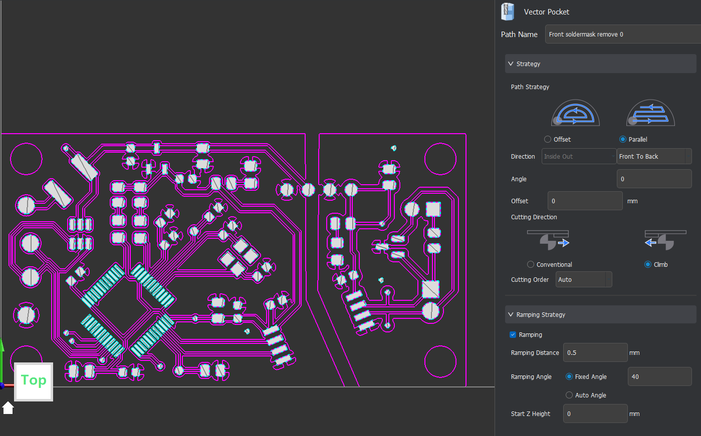
Start by loading the PCB back onto the fixture and secure it with a bit of double-sided tape. Using MakeraCAM, import front copper layer. This will create a layer with pads that we'll use as geometry for soldermask clearing. When generating the paths, I use the following settings for the job.
Additionally, end depth is 0.3 mm (can be changed to 0.5 mm is first run with 0.3 is not sufficient), stepdown 0.5mm, feed rate 400mm/min, plunge rate 200 mm/min, spindle speed 6000 rpm. I use "Parallel" strategy with ramping down because it helps avoid V-bit being in the point for too long, which could risk digging itself into the copper.
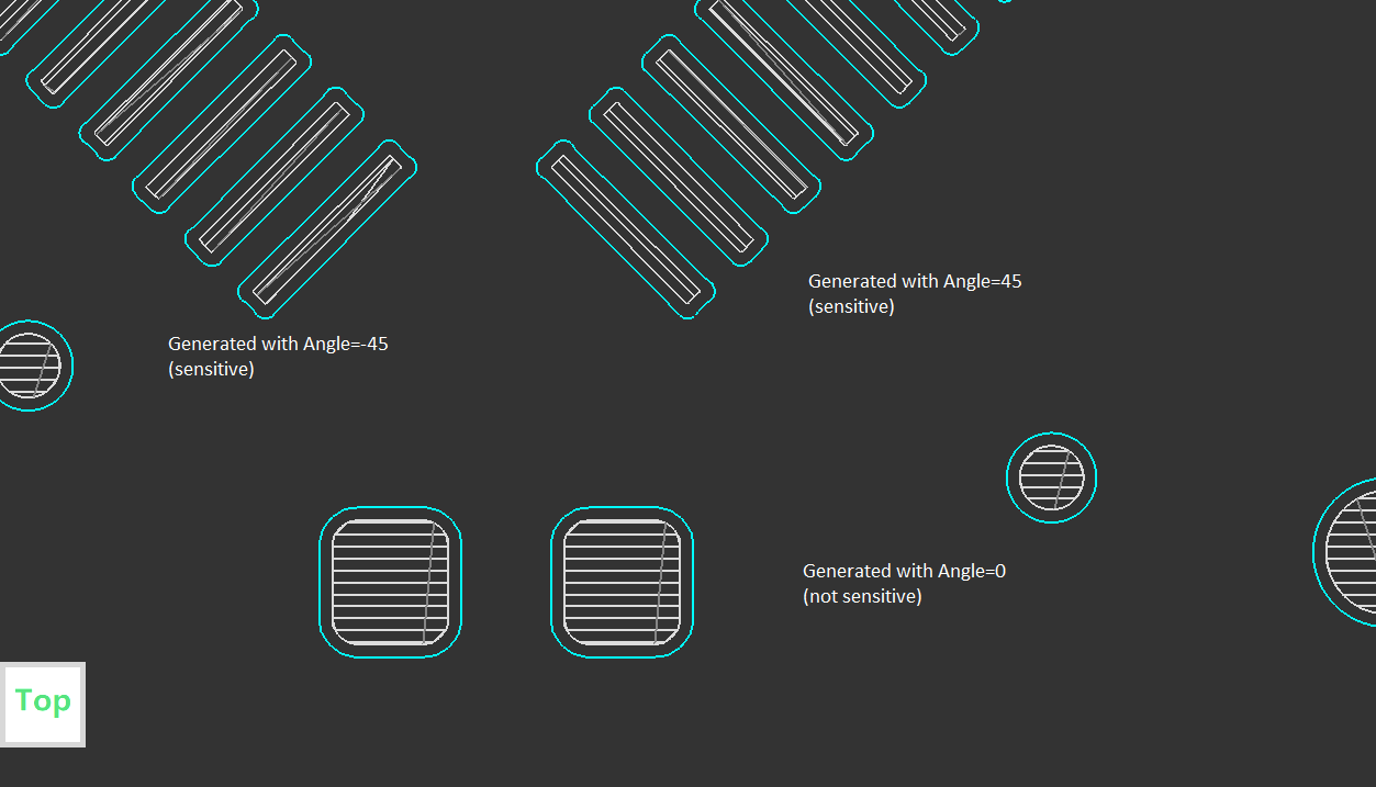
For the same reason, I will also generate paths that are aligned with some of the sensitive pads. In the picture above, 48 microcontroller pads are what I would consider sensitive. They are very easy to damage if spring-loaded bit passes over the same spot too many times. In that case, it's a good idea to create a special path just for that pad (or group of pads) where "Angle" field in the "Strategy" section is set to the angle of those pins to create a path in the direction of the pad, for example:
All 3 paths can be exported as one job form MakeraCAM and loaded in Carvera Controller.
Spring-loaded bit
To reliably use spring-loaded bit for solder mask removal, it's best to avoid built-in tool length offset measurement. Instead, start by changing to the solder mask removal tool using "Tool" menu in Carvera Controller. Then, manually calibrate Z=0 height by jogging the tool above the PCB, and slowly lower it down almost until in contact with the PCB. Insert a piece of paper between PCB and the tool and slide the paper while slowly bringing the tool in contact with the paper in increments of 1/0.1/0.01mm. Stop when the paper can barely move around and is not pinched by the tool. Now remove the paper and lower the tool for 0.1mm. Finally, lock the height as Z=0 using the "Z menu" in Carver Controller toolbar.
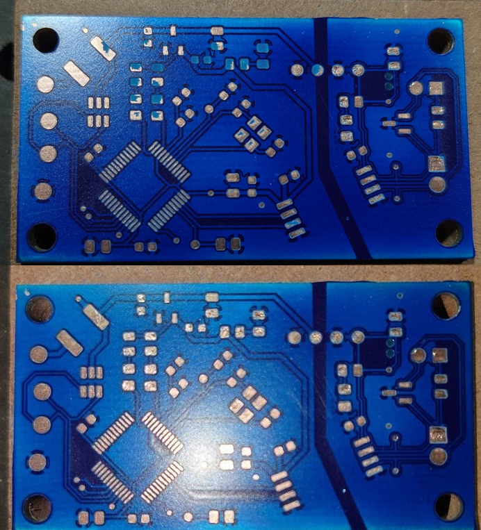
Run the loaded job to clear the pads. If not all pads are cleared after the first run of the job, simply rerun it again. This is because this process does not ensure even solder mask layer thickness every time. In this particular example, I apparently put a rather thick layer and had to rerun the job 5 times (first with end depth of 0.3mm, the rest with end depth of 0.5mm), after which I stopped and manually scraped away the remaining solder mask. I guess it had to fail since it was a demo :D
Picture above shows outcome after machining with few pads with partially removed solder mask (top), and outcome after manual removal with a tip of the tweezers.
7
Back copper routing/solder mask
Now it's time to repeat the steps for routing and solder mask on the back copper layer. Start by applying the double sided tape on the front side of the PCB, then flip it according to how the back copper layer was flipped in FlatCAM in step 2. Use align holes/pins to put the board back onto the fixture (see picture in step 4).
In Carver Controller, import .nc files for back copper isolation and copper clearing, then run them the same way it was done in step 4 for front copper routing. Finally, clean the copper surface (end of step 4) and repeat step 5 to apply the solder mask.
To generate path for removing solder mask, import back copper layer to MakeraCAM. First, ensure that stock size matches your PCB dimensions. Then select all graphics from both imported copper and pad layer, then mirror it (Select graphics -> "Adjust Object" -> Mirror). When mirroring, select "Stock Center" to mirror around the center of the PCB. Finally, confirm alignment using the align holes on front and back copper layer in Makera CAM.
Finally, repeat step 6 to generate, load and run the paths on the machine.
8
(Back) Silk Screen
(This step is heavily inspired by what's shown in this video)
If silk screen on the back of the PCB is needed, now is a good time to do it, board is already in the machine, and aligned. To make silkscreen, we'll use laser module on the carvera.
MakeraCAM setup
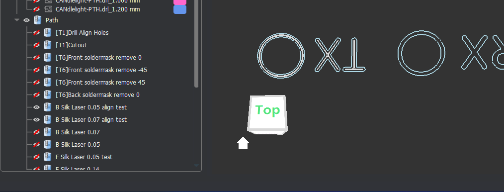
Start by importing silk screen exported from KiCAD into the MakeraCAM. Flip the silkscreen layer in the same way back copper layer was flipped in previous step (select, mirror with respect to the stock center). Ensure alignment by comparing to the underlying copper layer. To generate the paths, use "Laser Vector" feature in MakeraCAM, with the purpose of tracing the outline of silkscreen.
My experience with the laser is that it will produce very thick text, so for fine text (like component marking) the paths should be made as thin as possible without compromising the content. "Indent Distance (mm)" can be used to shrink the original vector when generating the paths for the amount specified. I found that for most of KiCAD designs, I split my silkscreen into 3 groups with different indent settings:
0.14mm - for the thickest text
0.07mm - for most of the text
0.05mm - for some of the lines, symbols and fine text
Each of these gets its own path as seen in the picture above, done at speed of 30mm/min, 3% power. Finally, all 3 paths with different indents can be exported in a single job to do all of silkscreen at once.
It might also be a good idea to generate a test path for only a single feature, to test the laser/CNC alignment. See below.
Preparing the PCB
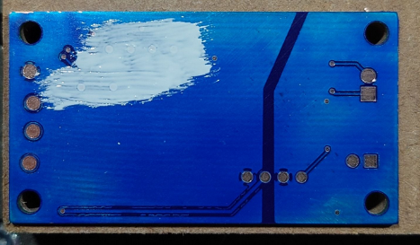
The process starts by applying a small amount of solder mask resin onto the PCB, then spreading it around with a brush into a very thin layer. The layer should be so thin, that you can almost see through it.
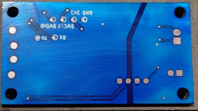
The low-power laser is then used to burn the silk screen into this solder mask layer, and the remaining resin can easily be cleaned away with an alcohol wipe.
As you can see in the picture above, this step will also require an extra step to ensure alignment between laser and the CNC. In my case, I had to offset X for -0.5mm and Y for 0.1mm - other machines might need different offset. It might be a good idea to test the alignment first on a single feature (e.g. TX pad in the picture above). before doing the rest of the silkscreen. This offset can than be added in Carvera Controller when defining work origin. In my case, work origin was changed from (2,2) to (1.5, 1.9).
However, once found, this offset seems to be very consistent and can just be copied over between designs. Offset is also the same regardless of whether it's the front or the back side of the PCB.
9
(Front) Silk screen
After completing the previous step, take the board out of the machine and flip it back so that the top copper layer is visible. Align the board back into the machine using the pins, and secure with a piece of double sided tape.
The procedure for front silk is exactly the same as for the back. Import silk screen layer into the MakeraCAM, split the silks screen into 3 layers with different indents and generate the paths. Import paths into the carvera controller.
Prepare the board by smudging a very thin layer of silk screen resin on top.
Ensure all areas where silk screen is, are covered with resin. Not like I did in the bottom right corner shown above :D. Then, if necessary, remember to apply the offsets found in previous set, to account for alignment between CNC and laser. Finally, run the laser job to burn in the silk screen. When done, clean the board with alcohol wipe.
10
Holes
Final step after the silk screen is to drill the holes. Import PTH files into MakeraCAM. This will result in multiple layers, one for each size hole your board has. Select each layer and generate the path for it using the right tool.
Export and run the job in carver controller, but remember to revert any changes to X-Y offset that might have been added earlier to account for offset between CNC and laser. In my case, this meant reverting from (1.5, 1.9) to (2,2).
 Vedran
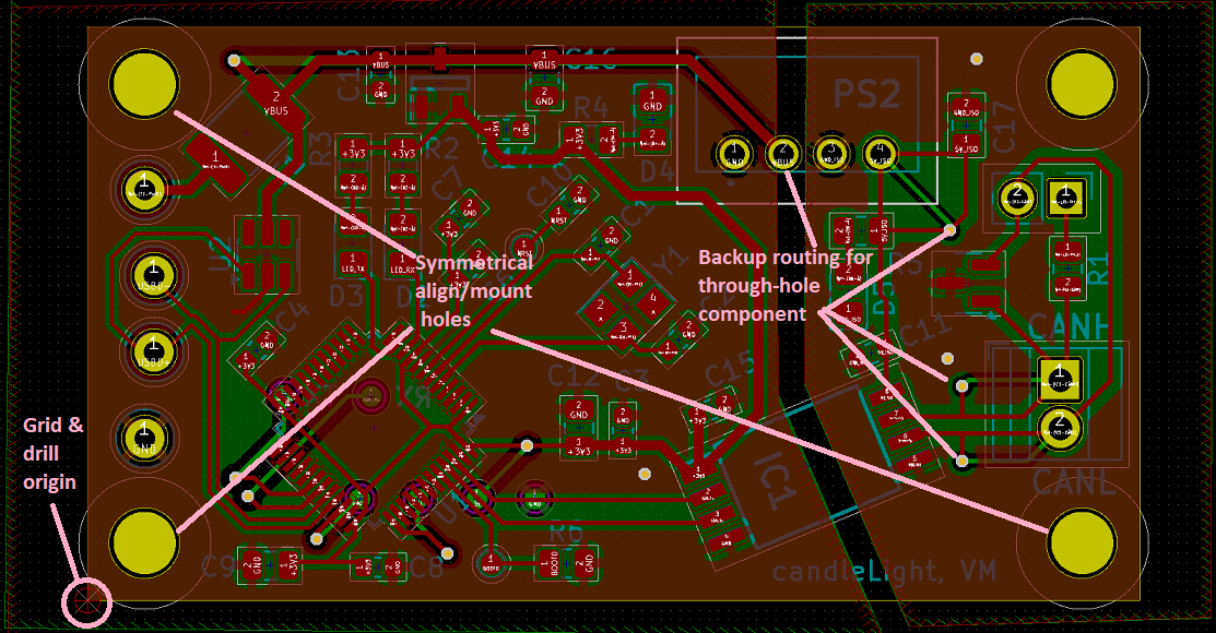


Discussions
Become a Hackaday.io Member
Create an account to leave a comment. Already have an account? Log In.