NandFarm Creator
-
Tindie time
02/27/2017 at 10:32 • 0 commentsThis project is now on Tindie: https://www.tindie.com/products/NandFarm/rfarmer-atmega256rfr2-24-ghz-zig
If anyone is interested, just make a request and I will produce the boards as soon as possible. (There is no need to make extra boards if there is no demand right?)
-
Hold up
02/21/2015 at 18:33 • 0 commentsDue to some personal matters I put this project on hold. I will release all the necessary informations/files in the "wild". The files are released under the beerware license.
If you have any questions regarding my work so far I would be happy to answer them.
Take care and have fun.
-
RFarmer v0.2 testing and antenna matching
08/08/2014 at 15:03 • 1 commentUnofficial rules for PCB trace impedance design:
1. You can never have too many vias.
2. Add more vias
3. Follow the datasheet instructions
4. Every PCB has different impedance so you may have different matching values for different PCB from the same batch.
5. You can never achieve more than 20-30% efficiency without a Network Analyzer that works at more than 2.5GHz.
6. If you are new at this, do yourself a favor and start with a dipole antenna.
7. Before you buy the matching components make sure their tolerances are in specs. A 0.2nH tolerance may not sound like much but it may be the difference between a working device and a pile of nerves.
As you may have guessed by now, I started testing the second version of the RFarmer. Once all the parts arrived I assembled the boards and I was ready to start tackling the matching circuit for the antenna trace. Imagine my frustration when I found out that the university where I can work with the network analyzer was closed for the summer vacation. What to do, what to do…
There must be some other way to match my circuit, right? Surely there is a hack-able way to do this, right? Right? ... No there isn’t! Not a full match at least.
Let’s talk some basics theory that was once learned and then forgotten.
In circuit theory we learned that maximum power is transmitted through a load when the resistance of the load is equal to the resistance of the source. This is DC. When we talk about AC, the same rule applies, but resistance is called impedance. Now, impedance varies with the frequency of the AC signal, and this is where it starts to be interesting. When you start working with high frequencies things start to get a bit voodoo. The main idea is this. The higher the frequency, the more interference you get from the things around the trace (other traces, vias, pcb dielectric, etc.) When you design a design a trace for an antenna, the main (only) impedance you wish to have is from the capacitor formed by the trace itself and the ground plane on the other side of the PCB. But things are not that simple. As you increase the frequency, stray capacitance (read inductance) will start to form between the trace and other traces near it. Even if you have a ground plane around the your trace, the lack of vias between the two ground planes will screw with the total trace impedance, leading to weird stuff like the device working when your hand gets close.
---To be continued---
-
BOM for RFarmer v0.2
08/06/2014 at 13:42 • 0 commentsIf anyone is intereseted, the BOM for the second version of the RFarmer is below in GDoc format. Sorry for the french. :)
https://docs.google.com/spreadsheets/d/1TEgQ4TBqWCJTCJENduR7_QOahBOAKJVGTIyD5ZP7G7g/edit?usp=sharing
-
BOM for RFarmer v0.1
07/24/2014 at 08:14 • 0 commentsIf anyone is intereseted, the BOM for the first version of the RFarmer is below in GDoc format. Sorry for the french. :)
https://docs.google.com/spreadsheets/d/1Xe9UU2TNJtcgu4D7nWzktiCj8DeVvA1QXRh-Goh0zBo/edit?usp=sharing
-
Before the RFarmer
07/23/2014 at 16:38 • 0 commentsBefore my ideea for the NANDfarm and the RFarmer; before via stithcing and impedance matching, there was The Base.
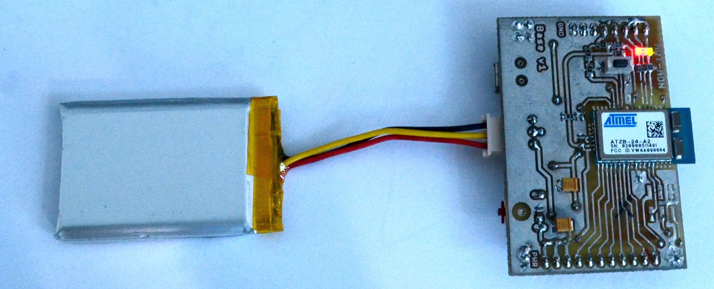
A few months ago (March?) a client asked me if I could build him a set of wireless interconected devices that can be controlled by a tablet. The ideea was nothing new. There are a lot of readily available boards/modules/chips avalilable on the market to do just this. The only problem was to find the right one. So I started looking into some readily available modules and settled on the ATMEL ATZB-24-A2 ZigBit module. It's small, it has an ATmega1281 inside and best of all it has an antenna.
After several hours in Eagle I fired up the CNC for drilling, heated the ferochloride shower and I was ready to start the production. I ended up making 3 main boards for the tests and a small USB-to-ZigBit dongle for the tablet. The main device looks something like this:
![]()
Aside for the passive components and the ZigBit module, I also used a Microchip MCP73871 Single Cell Battery Management Circuit and a FT230 for the serial communication. Usually I make my own boards because it's much faster than sending them to the fab. For this I use the CNC and the ferichloride shower available at a nearby FabLab.
All in all it turned out to be a very nice project so far. Now it's time to commence the programming.
Unfortnately, this is a work in progress, and I can not yet give the schematics or the BOM but I can happily answer all your questions. When other info is available, I will post it here.
-
RFarmer v0.1
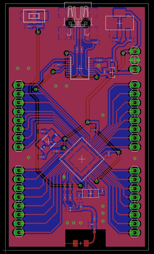
07/23/2014 at 15:58 • 0 commentsAs with every first version of a project, you are bound to find errors and problems. And I had a lot. Thinking back on it I can not imagine why I sent the board to the fab. This being said, I present to you my shameful first attempt at board manufacturing with the hope that maybe some people will learn from my mistakes.
The ideea was to start the prototyping process as cheap as possible. So first of all, I started ordering samples and after a few mishaps with the postal service here, I finally had some chips to work with. So I fired up Eagle and started to work on the schematic. After a few hours of work I was happy with the look of the board (at that time) and I started working out the prices and the aquirement of the component.
![]()
As anyone can see, there are a lot of problems with my design. First of all I did not put separate pins for device programming. So I had to connect all the necessary lines direcly to the PORTB headers. This worked for all the connections axept for the RESET. Luckily out of habbit I made the via holes for home PCB production (0.6 mm) and I was able to fit a small pin in them.
In my hurry to finish the design I completly forgot the basic rules for differential traces and impedance matching. I am ashamed. However, with the help of a good friend, and a Network Annalyzer from the electronics laboratory I managed to barely match the circuit which resulted in a whopping 10 cm of wireless range. I am still surprised it worked at all.
Aside from all the problems I had with this board, I am quite happy with the robustness of the small microcontroller. The single-chip sollution performed excellent even with all the short circuits bad connections, QFN hand soldering and impedance missmatching.
NANDfarm => RFarmer
Small, easy to use, cheap ZigBee developement board for the internet of things.