After ordering the internal base plate and front plate for the lens adapter machined in aluminium the camera can be finally assembled and the sensor to lens distance is easier to control.
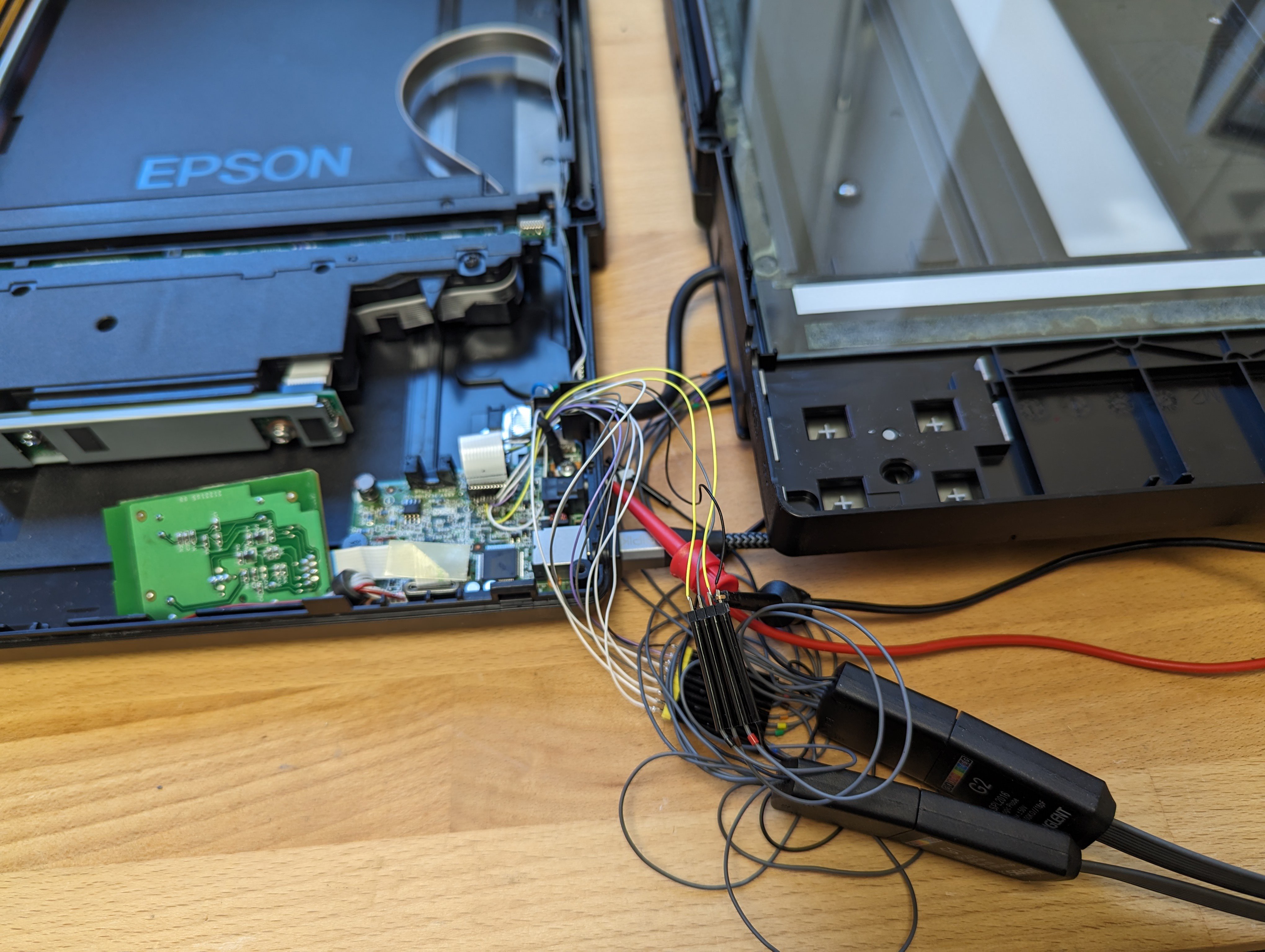
An nvme SSD was installed above the interface board just 1mm above the sensor assembly for storing images. The next version of the interface board got 1.5k pulldowns on each data line to clean up transitions and reduce the risk of glitches.
One big challenge is aligning the distances between the 2 sensors because if the second camera should help with focusing it must be on the same focus plane as the main sensor. Several different mounts have been printed and many more are to come until it is good enough.
Also the FFC routing and protection during movements is tricky.
The next big challenge is pixel shift correction and saving bitmaps directly from the application while capturing the image without external postprocessing.
As previously noted depending on the resolution mode the sensor has 3, 6 or 12 different active lines with different offsets to each other making an image appear blurry/shifted/jagged without correction.
For the correction a cyclic line buffer is used to avoid storing the full image in ram and instead the offsets are applied after every scanned line. It might be possible to speed this up further using parallel threads...
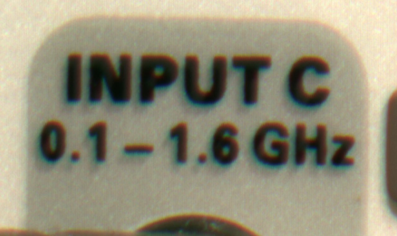
The big milestone is finally exceeding the resolution of commercial digital cameras by capturing a 21700x10000 200MP image:
And a zoomed section of the "Input C" of the frequency counter:
Note that there is still slight chromatic abberation and that every second line is slightly darker as the sub-lines seem to have a slightly different sensitivity.
As the final project should only run on a standalone computer the data needs to be acquired by a raspberry pi.
Using an RP2350 to generate commands and timing data was successful to read an image but the fullspeed usb interface is way too slow for the expected data rates of over 12MB/s.
The raspberry pi 5 has PIO state machines in the RP1 IO controller that can be used via PCIe using the new PIOLIB.
Getting the timing of the sync pulse right was a big challenge as the DMA transfer can take several milliseconds and it is not repeatable meaning after starting a line a random time passes until data is actually received and it is not possible to reconstruct colors from that.
Also the DMA transfer is currently too slow for full 16b resolution so only half the data is sampled at 8b resolution for now. This gets hopefully fixed with a later PIOLIB version.
After months of trial and error repeatable syncs have been achieved by filling and stalling the FIFO after each state machine reset, generating the sync pulse after syncing with the external clock in this SM when the DMA transfer starts reading this dummy data and then pulling the actual image data.
The first image may not look great but every line has the right color and you can see that it is a (blurry) image of a red flashlight on a table:
Red flashlight on table
Instruments on desk Realigned colour channels
With this image i think i am close to the right pixel pitch. Seems to be about 1.25µm at full resolution or an actual pixel distance within a line of 5µm which sounds reasonable. This image was taken in 1/8 resolution and has a certain analog feel to it.
With manually realigned colour channels it does look quite sharp already.
The most important step actually works. With actual image processing, pixel offset correction and a stiffer case it might even take good pictures.
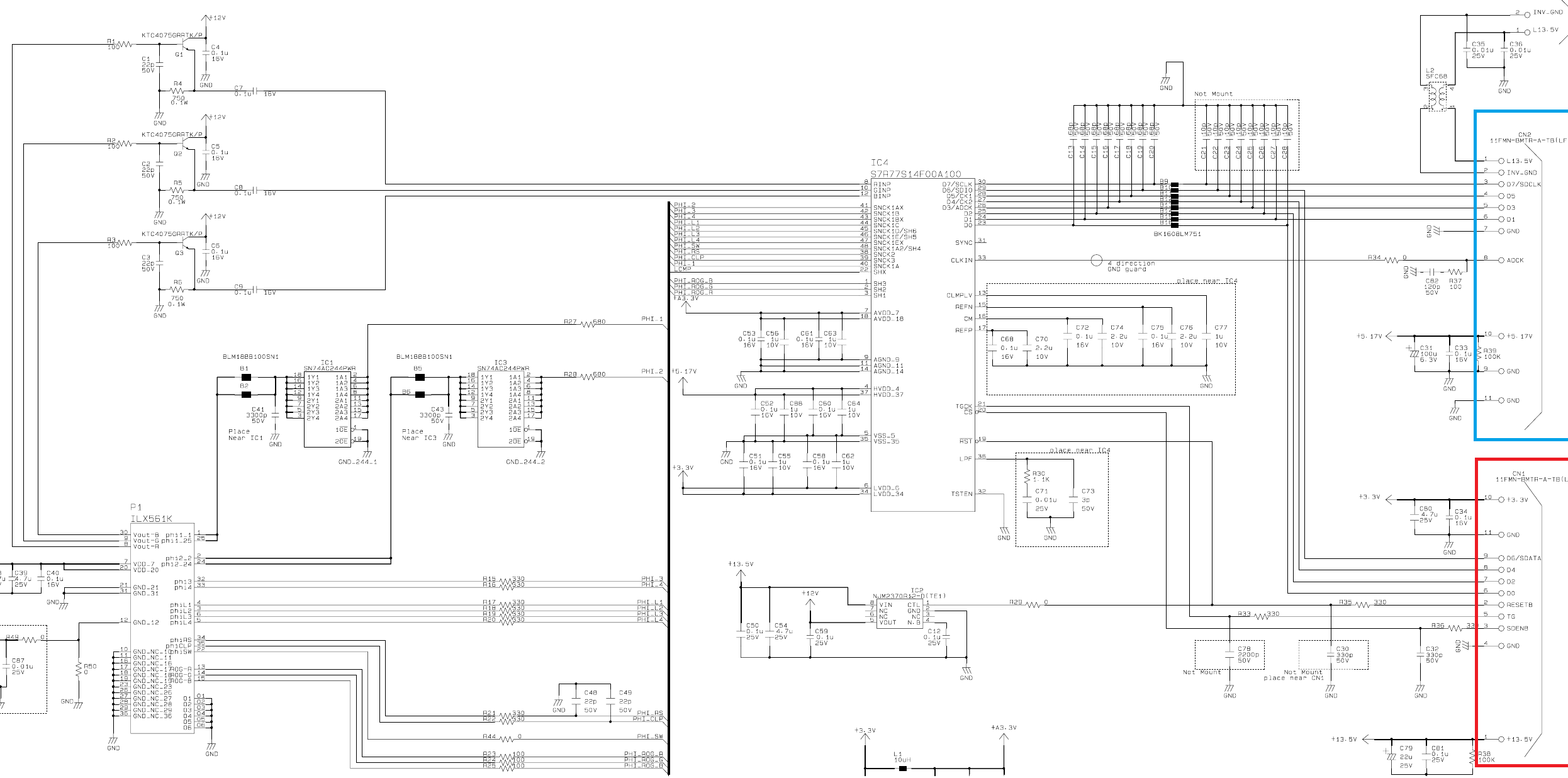
A service manual containing the schematic of a V200 using the same type of CCD was found which contains the labeled pinouts of the FFC connectors and part numbers of the CCD board.
Datasheets of the ILX561K CCD and Epson S7R77S14F00A100 are not public so some reverse engineering and data sniffing with a working unit is required.
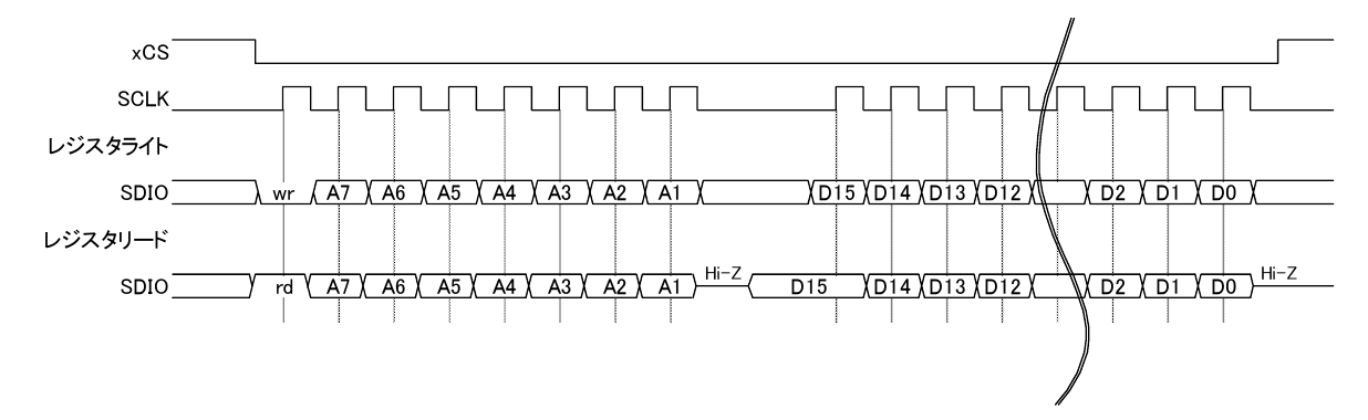
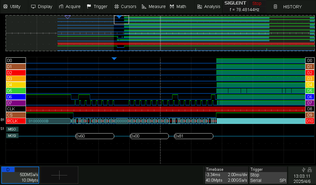
Note that the D7 and D6 pins are also labeled SDCLK and SDATA. These pins are used as half duplex SPI when the CS pin is low to transfer control data to the CCD interface and this is going to be very important to analyze for operation as this chip can not function unless the right CCD clock pin sequences are provided.
The now working v370 was modified by soldering wires directly to the FFC connectors and connecting them outside to a logic analyzer.
Data is being sent on 8 parallel lines with a 6MHz reference clock with data sent at both edges for a 12MB/s data rate and a TG line that seems to capture a new line and its frequency depends on the resolution setting. At the highest resolution it is only 46Hz transferring ~260000B (Full res sensor at 16b).
One notable command on the SPI control channel is 0x600081 and 0x600080. These start and stop outputting image data. The first bit indicates R/W operations. Because the data rate is low and i am intending to capture data using a PIO program i chose to use software bitbanging to read and write control data. The timing doesn't matter in this case. Comparing it to register maps of a similar chip (s7r77021) with a public datasheet the last bit seems to start the timing generator and data sampling. The register numbers are slightly different in this case but it was later found out that quite a few of the other registers seem to match.
A raspberry pi5 will be used to aquire image data due to its new piolib allowing PIO access to the RP1. After a lot attempts to decode colors from the image data of the existing scanner i noticed that the PIO DMA is not able to transfer data fast enough despite being connected via PCIe... Images were recognizable but it seems like the pi5 skipped at least every second byte with random pauses so the data is unusable to find out RGB offsets.
The TG pulse must be captured with the data to allow alignment later. Instead of capturing data at both edges of the clock only the first edge is captured and 3 samples with clock data are packed into one 32b buffer and decoded later. This did the trick and allowed a full line to be captured without missing too much data.
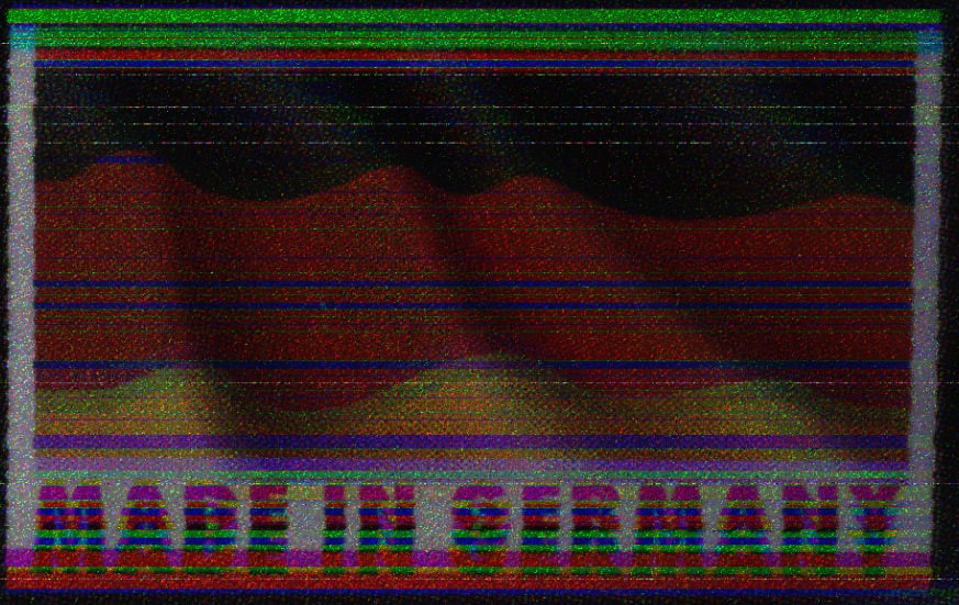
A color image of a random piece of paper could finally be decoded in 1200dpi mode which only contains the main lines and makes it easier to see. Yes there are random glitches and the colors are shifted due to the sensor layout but this is supposed to be a "Made in germany" icon.
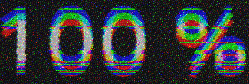
You can make out the flag and the text. On the "100%" text you can also see how the sensor moves its 3 distinct lines over the white text causing 3 ghost images.
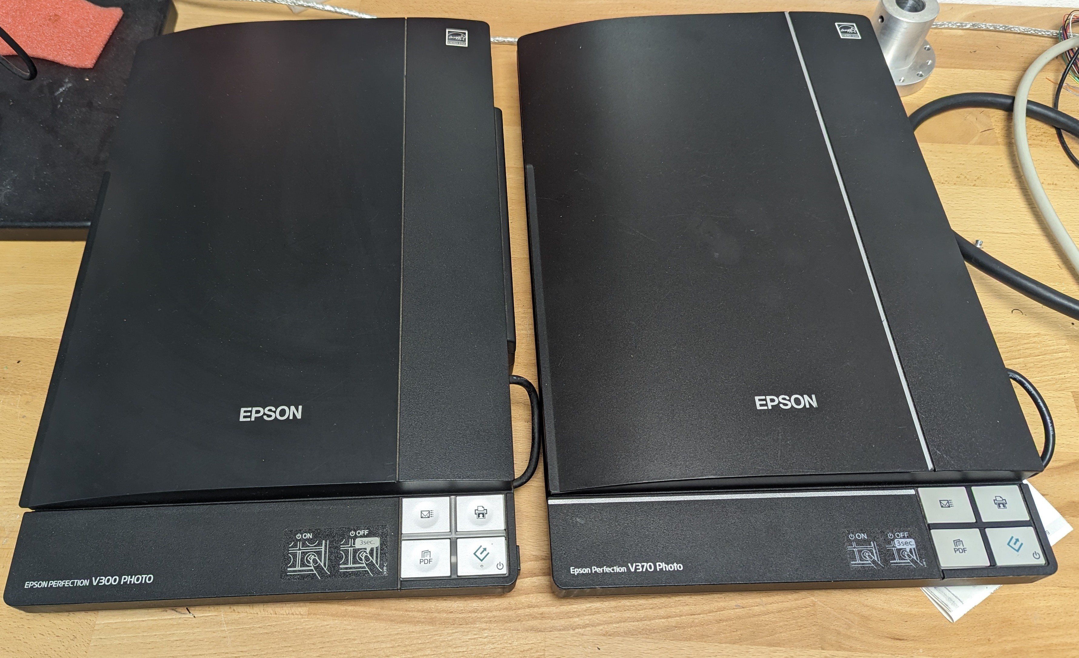
For this project 2 used scanners sold as defective were bought. 1x V300 and 1x V370.
The V300 still worked but lacked some accesories and is used as a reference.
The v370 had a broken usb port and even after replacement it still did not work so the s93c46 eeprom was dumped and transferred to the working V300 essentially transforming it into a V370 which advertises a higher resolution of 4800dpi.
The CCD assembly was kept intact for now in order to capture data from a working unit for analysis in the next log.
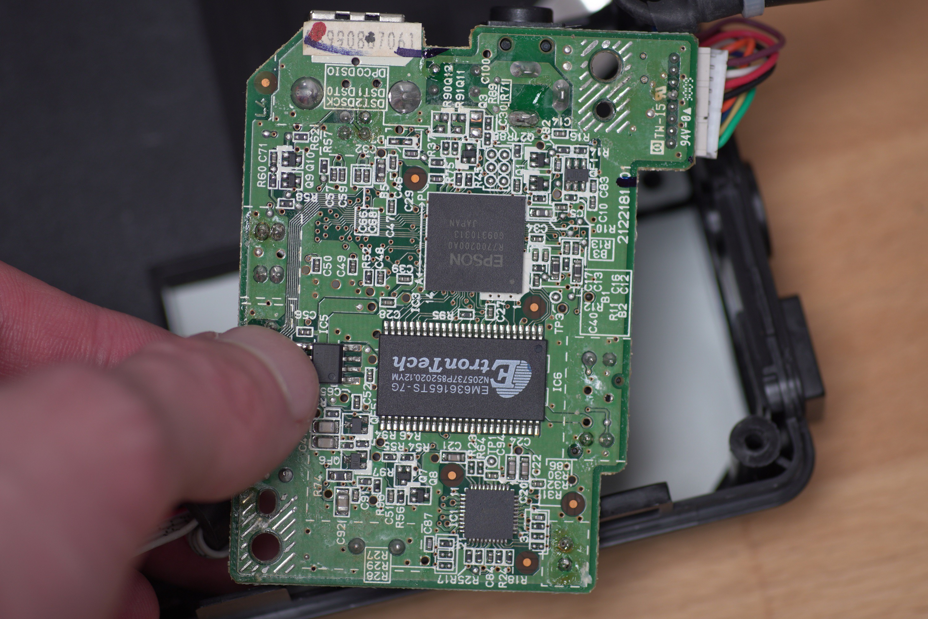
The main processor interfacing the CCD is actually not the one next to the USB port but a R7700200A0 on the underside with a big ram connected to it. The R720G000A0 seems to be only a HS USB interface for communication.
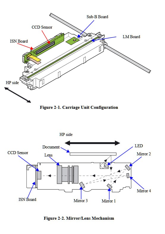
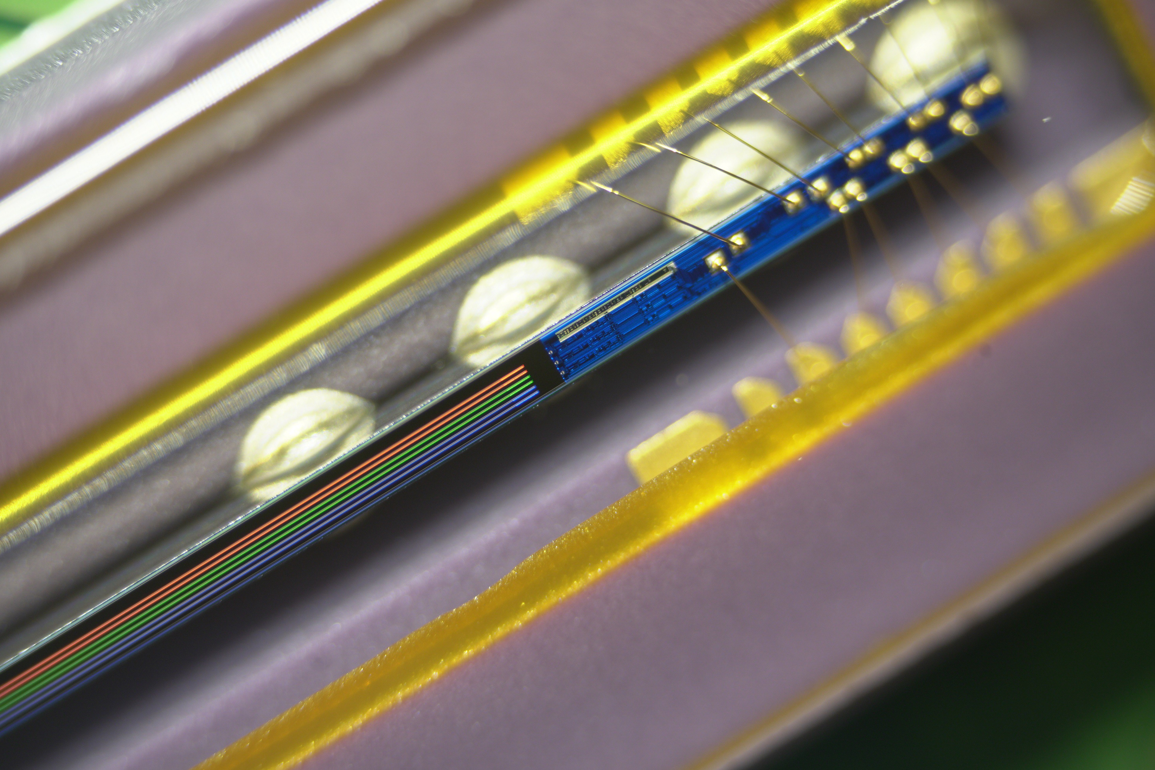
The Sensor used in these scanners seems to be the 12 line (RGB x2x2 Main+Sub line) ILX561K CCD with 122,400 total pixels. Because the lines are next to each other there is an offset of several pixels between them that needs to be corrected after capturing a few lines.
After startup these scanners home the main sensor axis and the light in the lid and if the homing fails or a white strip in the home position for calibration is not seen by the sensor the scanner enters a fault state. This means that if i were to just repackage this scanner into a different project the lid must be emulated or kept in some way to generate the homing pulse. It will not work without the lid attached or with the glass containing the calibration strip removed.
The sensor is split into 12 lines. Each color has 2 groups of 2 lines each for 4 lines per color. It is likely comparable to the 6 line ILX585K where a public datasheet is available. The pixel pitch there is (likely) 4µm with 48µm? between main lines and 8µm? between sub lines for an effective 1µm pixel pitch of the staggered pixels in this sensor.
Because the ILX561 sensor has 2 main lines per color the distance between colors is likely double the distance of the ILX585K. This will be important to know later during image processing.
 Yannick (Gigawipf)