 Bud Bennett
I received an order of 5 USB-C trigger boards a couple of days ago. The available voltages from the trigger board are 9V, 12V, 15V and 20V. I have two bona fide USB-C adapter/chargers, both from Samsung, one is 25W and the other is 45W. I also have two clones of Apple adapters with USB-C jacks and a USB-C adapter for the Raspberry Pi 4. The first thing I did was to plug a trigger board into the USB-C port of my desktop computer. The little blue LED on the trigger board did not light up and the voltage output read 5VDC. I expected this behavior.
Then I connected the trigger board to the 45W adapter. The LED indicator lit immediately and the trigger board put 9VDC at the outputs. The problem with this is that the trigger board is set for 12V output. I'm a bit confused at this point so I plug the trigger board into the 25W adapter. The LED indicator eventually lights up after maybe 5-10 seconds. The output voltage is 12VDC. The two Apple clone adapters both light the LED immediately and put out 12.4VDC. The RPi adapter only puts out 5V. Now I'm really confused as to what is happening.
I trolled the internet as to what the issue could be but found nothing useful. At this point I have zero trust that the trigger board will output the correct voltage and it dawns on me that the circuit I designed probably won't survive in the wild without some improved robustness. The VREG daughter board must not fail or damage the expensive core probe circuitry if/when 20VDC is applied to its supply pins!
When I was designing circuits for a living I worked with some very experienced people (you might even call them legends.) They taught me a couple lessons:
- The best circuit designs are the ones that apply to the broadest range of applications.
- Sometimes a circuit's survival is more important than its performance.
The PCB is tiny, only 13x13mm. It is also a DIY project, so 0201 components are out of consideration. I figure I could add a single SOT23 (not the difficult to solder SC70) and 2-3 resistors if most of the resistors could be 0402 size. After toiling away for a couple of hours on LTSpice I finally had a Eureka moment -- using another TL431/TL432 as a reference/comparator in the following circuit:
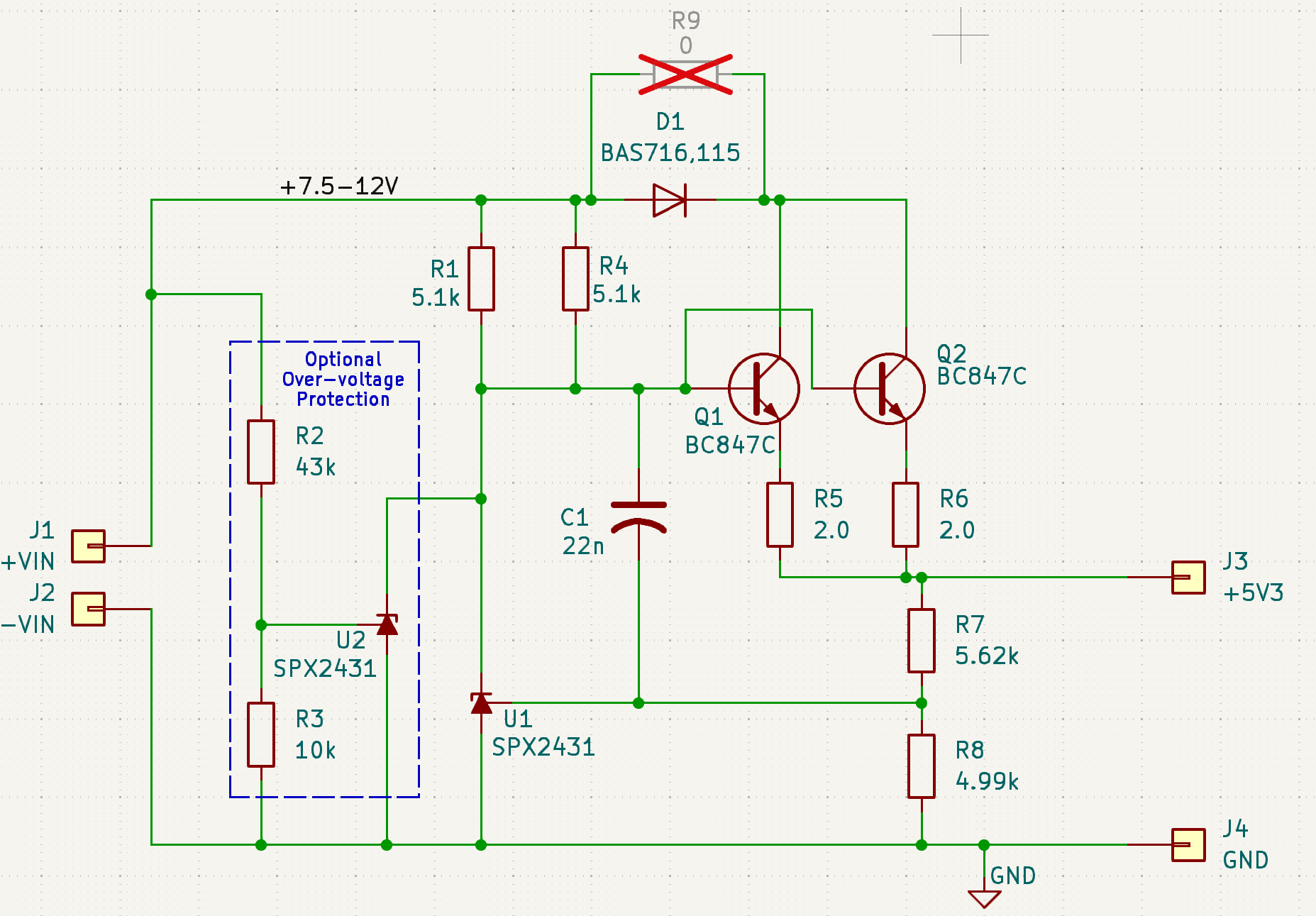
This worked like a charm in LTSpice with behavioral models for the TL432. When the input voltage exceeds 13.2V the voltage at the REF pin of U2 exceeds 2.5V, and U2 will draw a lot of current from its cathode pin, effectively shutting down the output voltage at J3. U1 will attempt to compensate, but all it can do is reduce its current until it goes to zero. R4 is used to share the current through R1 and keep the power dissipation below the 100mW limit for 0603 resistors. This action saves Q1 and Q2 and R1 from burning up when 20V is applied. D1 protects the components against reverse polarity inputs.
Then the gloom settled in as I realized that the behavioral models might not exhibit all of the correct behavior of the TL432. Here's the problem: Where is the current coming from to power U2? I measured pA of current into the anode of U2 using the first behavioral model from TI. The second SPICE model from TI sucked a whopping 1uA from the anode pin until it began to override U1. Still not correct.
TI publishes the anode current vs voltage in its datasheet:
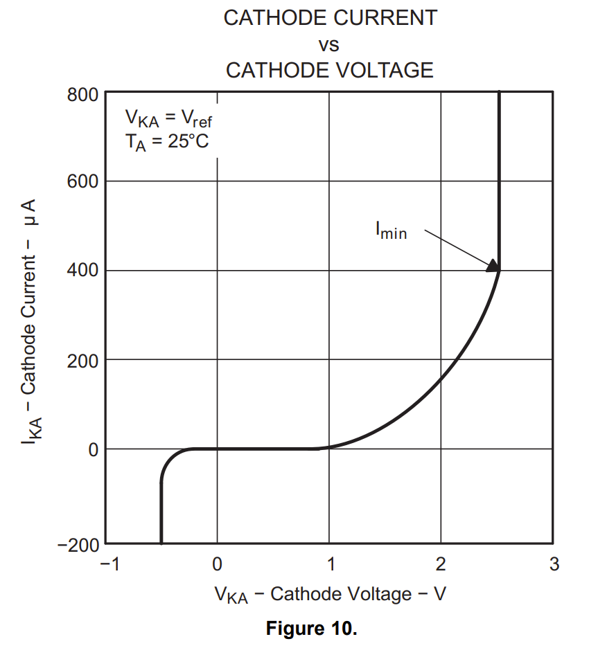
That's not really helpful. Fortunately, TI published a schematic, with values, of the TL431 in the datasheet:
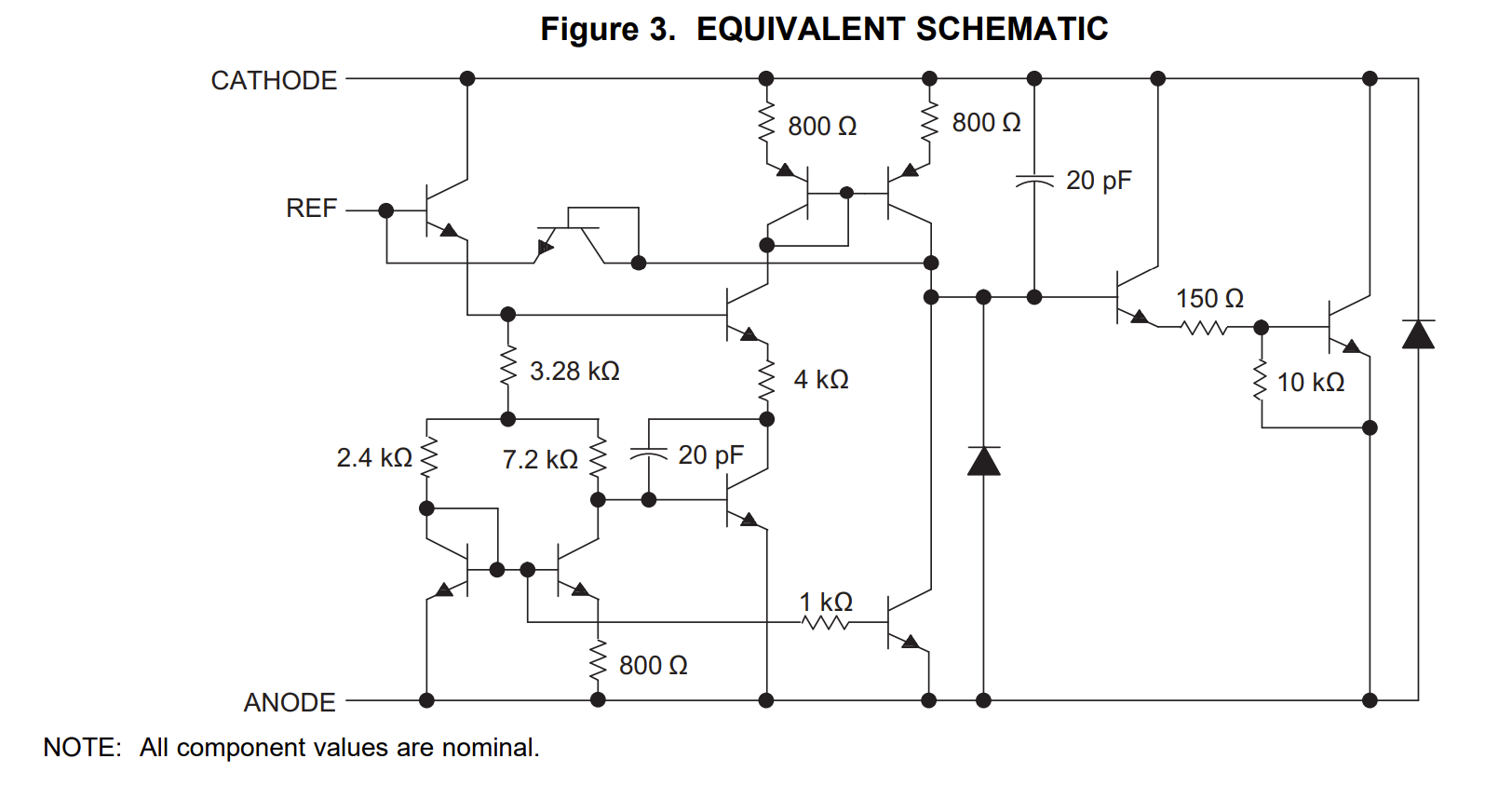
And I created a schematic to imitate U2 in LTSpice:
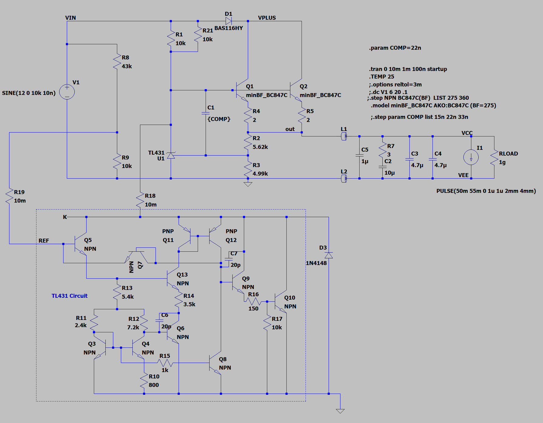
I used generic LTSpice NPN and PNP models which forced me to change R13 in order to get the circuit to regulate at 2.5V. Now I expected the currents at REF and K to be more realistic (but probably not perfect.) A DC sweep of V1 confirmed it:
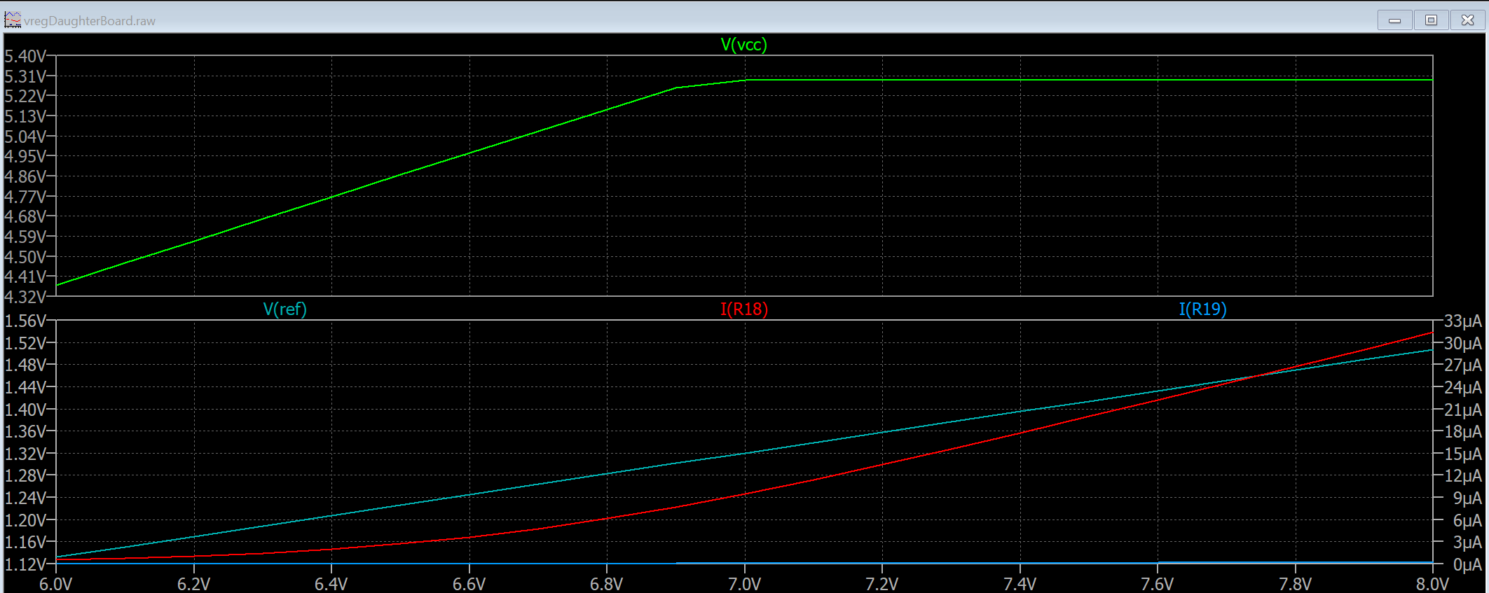
R18 monitors the current into the anode and R19 monitors the current into the REF pin. There's no contest...nearly all the current is going into the anode. This gives me some confidence that the over-voltage protection won't interfere with the normal operation of the regulator until the input voltage exceeds 13V:
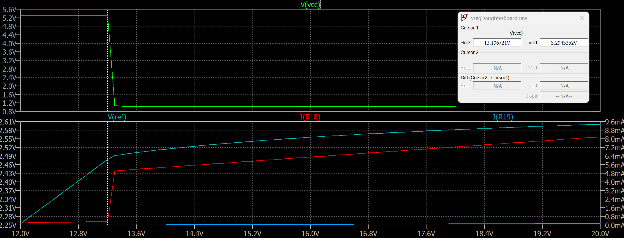
And that is apparently correct -- the over-voltage monitor doesn't impact the output voltage until the input voltage exceeds 13.2V. Note that the output of the regulator drops to about 1V. That is because U2 requires some voltage across its anode in order to continue to function.
I ran several simulations to determine the performance of this circuit.
- The values of R1 and R4 should be raised to 10k with input voltages of 12V. This keeps the power dissipation lower in normal operation and limits the dissipation with 20V input to less than 33mW in R1 and R4. With R1, R4 = 5.1k, the power dissipation increases to 66mW at 20V, which is still acceptable for a 0603 resistor.
- Q1 and Q2 are the big power hogs. They will dissipate 200mW/each when dealing with 12V inputs. They will get hot -- around 110C.
- The compensation capacitor, C1, is awfully large. It is OK though because the big tank capacitors across the output and opamps will take care of any fast transients. I'm trusting the SPICE behavior models to properly emulate frequency response (I used 3 different models) but can't help wondering about what the real circuit will need for compensation.
- If you need to use an adapter that outputs 7.5V-9V then the standard issue TL431 requires too much current (1mA) in order to regulate. This lowers the values of R1, R4 and causes them to exceed their power dissipation limits if a 20V fault occurs. There are many (~75) lower current alternatives to the old TL432 that require less than 200uA to operate.
All of this protection was put in place because I can't trust the trigger board to produce the correct output with various USB-C adapters. If you have a dedicated adapter or non-USB-C adapter, then all of that protection can be depopulated.
There are two tables on the VREF daughter board schematic: one for suggested values for R1, R2, and another table for suggested lower current alternatives to the TI TL432. I also suggest that a 9V adapter (or trigger board set to 9V) be used to power the probe. A 12V adapter will cause about 400mW of dissipation vs. only 220mW with a 9V adapter.
Note: The TL432 is used in this circuit. It is the same device with a different pinout than the TL431. The SPX2431 is in my inventory, and has the same pinout as the TL432, so that pinout is used. I'll put a note on the schematic too.
Discussions
Become a Hackaday.io Member
Create an account to leave a comment. Already have an account? Log In.
Another novel idea and excellent solution to the problem. Well done Bud!
Looking forward to see the circuit work in real life conditions, but I have very little doubt that you've got it nailed.
Are you sure? yes | no