Use a small (<30W) GaN USB-C power adapter. At first, I purchased these adapters from Amazon. They are ridiculously cheap. They worked for the 100MHz probe but did not deliver the required 20V for the 10MHz probe. I purchased this adapter for the 10MHz probe, which works well, and would suffice for all of the probes. Paul opted for a 100W USB-C power adapter that was more suited for laptop computers than phone charging, but even the phone chargers he tried produced too much switching noise. He also tried cheaper adapters, but settled on a 30W GaN power adapter as his final choice -- they have the least amount of switching noise (with a higher switching
frequency) that the on-board filters on the probe can eliminate.. See Paul's blog for details.
There are only two trigger board voltages that make any sense, depending upon your choice of diff probe BW: 9VDC for the 100MHz probe body, and 20VDC for the 10MHz and 1MHz probe body. Choosing 12VDC will result in much higher power dissipation (and heat) with no benefit whatsoever in performance.
Pair the 100MHz probe body with the buck converter daughter board and set the USB-C trigger board to output 9VDC. I think this will yield the lowest power dissipation and coolest operation of the probe. I did not see any evidence that the 2MHz switching noise of the buck converter was visible in the diff probe output. Alternatively, you could pair the probe body with the SOIC daughter board, and trigger board set to 9VDC, if you are concerned about switching noise.
Pair the 10MHz or 1MHz probe body with the depopulated version of the discrete VREG daughter board, or the SOIC8 daughter board. Both of these DBs have excellent tolerance (<0.5%, best case), line and load regulation, and low power dissipation. The depopulated discrete VREG daughter board looks like this: If you don't require reverse polarity protection, then substitute R9 (a 0603 short) for D1.
We don't recommend using the mini USB daughter board or the SOT89 daughter board. The raw voltage provided by a generic USB power adapter may cause the offset voltage of the probe to fluctuate. I found the SOT89 XC6216 LDO to have poor line/load regulation compared to alternatives.
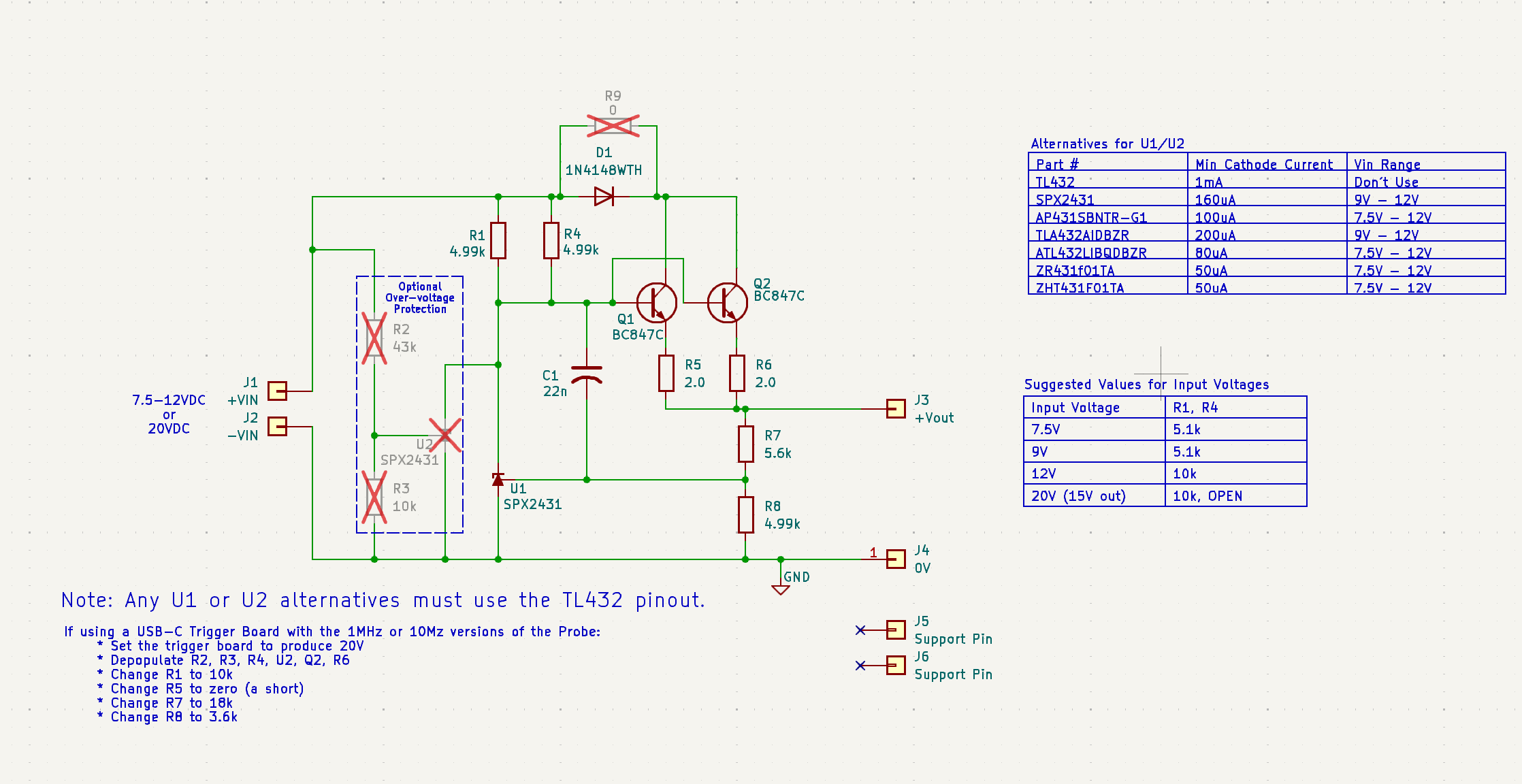
Battery Power: It is much easier to just go with USB-C, but if you insist on opting for battery power, then there are options. For the 100MHz probe Bud would recommend two 4.2V Li-Ion cells and then probably go with the Discrete VREG daughter board since it will work with 6.5V input voltages. The discrete VREG can prevent disaster if you apply more than 12V or reverse polarity. Here's the fully populated discrete VREG daughter board schematic:Paul implemented a battery power scheme with a 9V alkaline cell, again using the discrete VREG daughter board. For the 10MHz/1MHz probes you can stack two 9V alkaline cells, or use a stack of five 4.2V Li-Ion (21VDC), with a depopulated discrete VREG daughter board.
If you are going to build the 10MHz/1MHz versions and you desire more differential input voltage range you can tweak the SOIC8 daughter board to output more than 18V, which would yield +/- 90V. The SOIC8 daughter board uses an LDO that requires much less headroom than the discrete VREG daughter board. Be careful though, there will be more stress on the bypass capacitors. (If you really want to go crazy, the max supply voltage of the OPA2810/OPA810 is 27V.)
Lead Inductance. See my log about this for more information. If you are going to add some clip leads, make sure to add the appropriate series resistance in each lead. I use 220 Ohm resistors in each of my 100mm clip leads. The other added benefit to the resistors is that they will decrease the probe's loading on a circuit at high frequencies. I calculate the reactive load from a 2.5pF input capacitance is about 640 Ohms. The 220 Ohm lead resistance, along with the lead inductance will likely add another 300 Ohms, for about 1K Ohm at 100MHz. That's 10X better than the 100 Ohm loading from a 15pF scope probe.
Modifications. This architecture lends itself to endless variations in differential voltage gain, differential and common mode voltage range, noise performance, etc. You are on your own if you go down this path. Be aware of the limitations of the layout and the component ratings. You're probably not going to get a 0805 resistor that will withstand 200V, let alone 1kV. If you need more common mode voltage range then you're going to need a different layout with different (and probably more) components to withstand the voltage.
 Bud Bennett
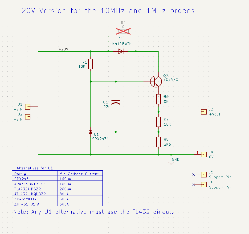
Discussions
Become a Hackaday.io Member
Create an account to leave a comment. Already have an account? Log In.