 Jake Robinson
Overview
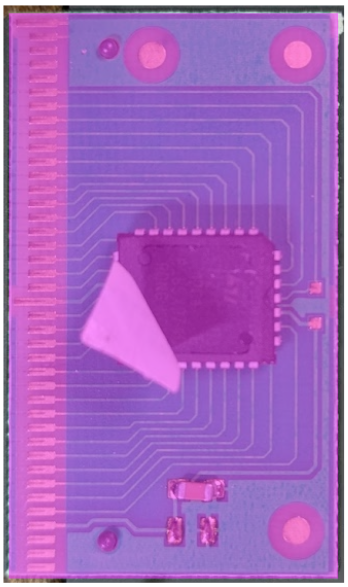
Quick note on a process I am testing to quickly fabricate a PCB using the vector graphic tool Inscape. This log covers tracing a single-sided PCB from the cartridge pictured below. The goal is to take an image of the board and convert it into a file I can send to a board house without doing a traditional layout.

The picture is not optimal (the sticker is in the way and there are still components on the board) but this test is simple enough that those things should not be an issue.
Process
I am using Inkscape to trace the PCB and a set of calipers to measure the physical board.
To start, I imported the picture into Inkscape and drew a box with the same dimensions as the actual PCB. I used the box to scale the image to its real size. The camera introduced almost no noticeable deformation, which is a good sign for this workflow.
I created a new layer for the components and another for the copper layer. This should let me export the copper layer to KiCad later.
The result looks like this

There is a pad on back of the memory component that is not shown here. I will need to add that before moving into kicad.
Conclusions
This first pass shows that tracing a PCB image with Inkscape seems to work well for a small single-sided board with only SMD components. The scaling step was straightforward and the lack of distortion makes the method viable. Next, I want to finish the copper layer and test exporting it into KiCad to see if it can go straight to a board house like OSH Park without any additional layout work.
Discussions
Become a Hackaday.io Member
Create an account to leave a comment. Already have an account? Log In.