 Jake Robinson
Short update for today.
I finished the Inkscape trace and started a process of importing the design to Kicad. Kicad has a tool that converts a picture into a PCB footprint. The idea is to import the Inkscape picture into the tool and convert it into one large footprint.

I exported the trace layer from Inkscape as a PNG at 300 DPI. I used this PNG in the image converter.
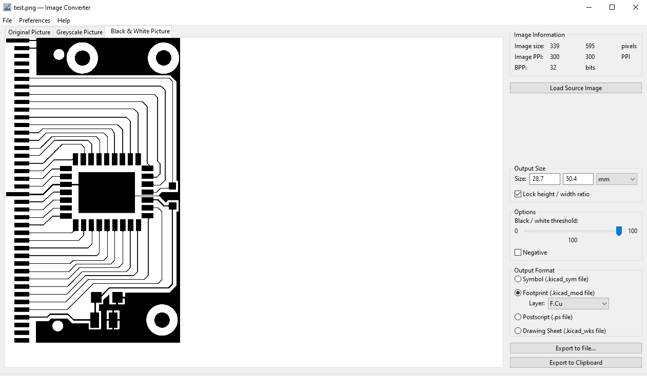
This seemingly works as expected. There are some options to configure such as the Black/White threshold and negative output. I bumped the threshold slider all the way to 100. I also verified that dimensions looked correct. I exported this as a kicad footprint with the F.Cu layer selected.
To test the conversion, I started a new project and when directly into PCB layout, imported the footprint and placed it in the design. Zoomed out the footprint looks accurate, but as I zoomed in I could see some approximations in the shape.

This picture shows the issue. Its interesting how some of the geometry is shown with sharp edges while others have been rounded. The traces are also a little thinner then the original. Not sure where this is cropping up but I plan on looking into this issue for the future. I'm sure someone else has looked into this problem.
Another issue was defining the pads.

I expected this to be a issue but I'm not certain on the fix for this one. This will be the other topic of research for next time.
Discussions
Become a Hackaday.io Member
Create an account to leave a comment. Already have an account? Log In.