 Edward
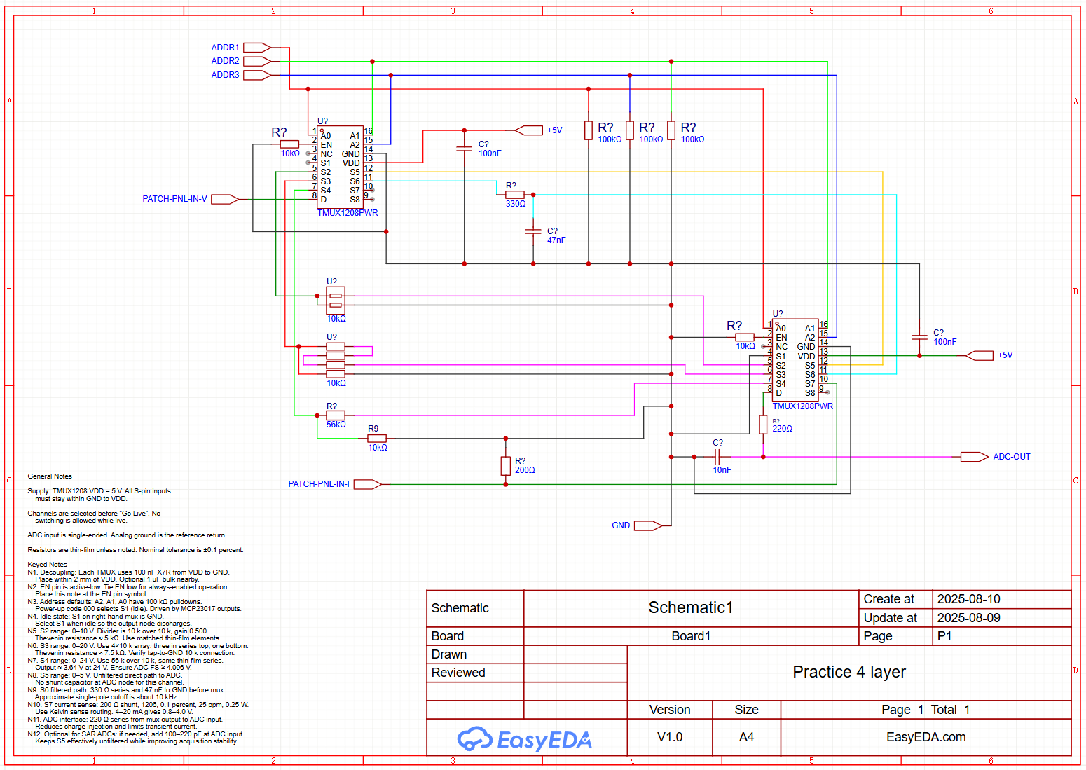
I’ve been wiring up a small analog front-end that lets one ADC read a bunch of different field signals: DC voltages in a few ranges, a filtered line, and a 4–20 mA current loop. The trick is a dual TMUX1208 setup so voltage and current paths switch in lockstep with the same address.
Architecture at a glance
-
Two TMUX1208PWR analog muxes, VDD = 5 V.
-
EN is tied low (active). No live reconfiguration; the UI locks the channel once you hit “Go Live.”
-
A2:A1:A0 come from an MCP23017. Three 100 kΩ pulldowns force a safe power-up state.
-
S1 on the output mux = GND, so the ADC node discharges when idle.
-
220 Ω series between mux-out and ADC-in to tame charge injection.
Channel map
-
S2 — 0–10 V: 10 k/10 k (½). Thin-film, 0.1 %.
-
S3 — 0–20 V: ¼ divider using a 4×10 k thin-film array: three in series for the top, one to ground.
-
S4 — 0–33V: 56 k/10 k (≈0.1515). Both parts from the same thin-film series (Yageo RT) to keep ratio drift down.
-
S5 — 0–5 V: unfiltered straight path for clean, fast measurements.
-
S6 — filtered line: 330 Ω + 47 nF to ground (~10.3 kHz) before the mux for EMI/noise.
-
S7 — 4–20 mA: 200 Ω shunt (1206, 0.1 %, 25 ppm). That gives 0.8–4.0 V at the ADC.
Parts choices that mattered
-
Resistor quality: thin-film 0.1 % / ≤25 ppm everywhere that sets gain.
-
S2 uses a dual 10 k array; S3 uses a quad 10 k array for perfect 3:1 + 1 matching.
-
S4 uses RT0603BRD0756KL (56 k) and RT0603BRD0710KL (10 k).
-
-
Decoupling: 100 nF right at each TMUX VDD, plus ground-via at the cap pad.
Gotchas and fixes
-
Facepalm moment: I initially dropped the 100 nF on an S-pin instead of VDD. That accidentally AC-coupled a channel to 5 V. Moved it to VDD↔GND where it belongs.
-
Pulldown current: 10 k on A0–A2 wasted current; moved to 100 kΩ since the expander drives push-pull.
-
S3 wiring: easy to forget the bottom 10 k to GND at the tap when using arrays—fixed and verified (VIN→30 k→tap→10 k→GND).
Why the “no live switching” rule
I don’t need rapid channel hops, and preventing changes after “Go Live” avoids odd transients or user error. With static selection, even the slowest divider path has all the time it needs to settle, and S5 stays truly unfiltered.
PCB plan
-
Keep the ADC node tiny; place TMUX chips nearby.
-
Kelvin route the 200 Ω shunt.
-
Put the S6 RC right at the S6 pin.
-
If the quad-array stock gets thin, the layout fits two dual 10 k arrays as a drop-in backup (3 in series for the top, 1 for the bottom).
Bring-up checklist
-
Power smoke test, then verify 5 V and idle S1→GND at ADC-in.
-
Program MCP23017 → default 000.
-
Range checks:
-
S2: 10.00 V → 5.00 V
-
S3: 20.00 V → 5.00 V
-
S4: 33.00V → ~5.00 V
-
S7: 10.00 mA → 2.000 V
-
-
Store one-point gain trims per range.
Next up: route the board, save it as a reusable circuit, and move on to the analog outs.
Discussions
Become a Hackaday.io Member
Create an account to leave a comment. Already have an account? Log In.