Close
0%
0%

RacKITT - Rack mount scanner bar using op-amps

Knight Rider scanner lights for your server rack - analogue style!

Similar projects worth following
Recreating the iconic scanner bar from Knight Rider in a rack mountable format, and learning analogue design at the same time - no microcontrollers here! Aiming to complete in time for the 1Hz challenge, setting the lights to scan from one side to the other every (approximate) second.

LED scanner lights are usually quite simple to make - an Arduino, some addressable LEDs and a dusting of software. However, as a maker who learned in this digital domain of electronics, the design of analogue circuits is a skill which has eluded me. Perhaps in the same vain as "could've used a 555", the idea of using an entire processor and software stack feels overkill, when transistors and op-amps could do the job just as well. 

Inspired by a colleague to deck out a server with the KITT scanner bar from Knight Rider, I challenged myself to design a 1U sized analogue implementation of the device, to gain a basic understanding of analogue design. This included emulating the slow "fade out" of old incandescent bulbs, as just switching an LED on and off isn't nearly as cool, and re-discovering a handful general design principles from issues stemming from my own poor decisions during design and assembly!

Adjusted for a scan interval of 1s from one side to the other, it becomes eligible for the Hackaday 1Hz challenge, giving a motivation (and deadline) to actually complete it! 

I'd like to give special thanks to:

  •  My dad for the frankly absurd amount of quite fiddly soldering he had to do to join all of my circuit boards together, in addition to having to separate them all manually and putting everything together for the first test run.
  • For my friend who 3D printed a replacement potentiometer knob with less than a days notice when I found out the one I had bought wouldn't fit.

Table of development logs, ordered chronologically:

#Log (hyperlink)
1Motivation
2Concept
3LED Module Schematic Design
4Control and Power Module Schematic Design
5Circuit boards!
63D printer spacers and LED enclosures
7First light
8Decorative components
9Tuning for a 1 second sweep time
10Lessons Learned (or "how I should've done it")

RacKITT_schematic.pdf

PDF Export of main electronics schematic

Adobe Portable Document Format - 2.72 MB - 08/13/2025 at 22:34

Preview

RacKITT_PCB.pdf

PDF Export of main electronics PCB layers

Adobe Portable Document Format - 3.70 MB - 08/13/2025 at 22:34

Preview

RacKITT_jumpers_schematic.pdf

PDF Export of interconnect boards schematic

Adobe Portable Document Format - 138.31 kB - 08/13/2025 at 22:34

Preview

RacKITT_jumpers_PCB.pdf

PDF Export of interconnect boards PCB layers

Adobe Portable Document Format - 315.93 kB - 08/13/2025 at 22:34

Preview

acrylic_cuts_labels.pdf

PDF export of labels and cutting/drilling guides for acrylic front panes

Adobe Portable Document Format - 19.38 kB - 08/17/2025 at 20:30

Preview

View all 26 files

  • Lessons Learned (or "how I should've done it")

    Eontronics08/10/2025 at 12:08 0 comments

    Following the rare occasion of actually seeing the project through to completion, there were a number of occasions along the way which lead me to question "why on earth did I do it this way???". I'll try to capture some of those moments here, as a warning to (mostly) myself and others to consider in future projects.

    That said, electrically, everything worked surprisingly as expected, so most of the problems listed below are due to poor design choices, rather than simply not knowing something:

    What didn't go well:

    • To save on PCB manufacturing, I created many small PCBs which could be tiled into one to be eligible for discounted PCB prototype pricing. 
      • As it turns out, the cost of convenience when it comes to ordering PCBs overseas is not much, and a huge amount of effort could be saved from instead designing 1 or 2 big PCBs that can be installed directly, and would probably end up being cheaper, when considering the cost of parts for workarounds needed to get the first method to work. 
      • In my case, using tiled PCBs meant: Having to design and order a whole new set of PCBs to bridge between them, as wiring them manually was next to impossible to do. This also meant buying more headers to attach them with, and then having to hand solder 480 connections to assemble everything!
      • For comparison, ordering a single monolithic board would have added ~£10 to the original order cost, and the only extra soldering required would be 5 flying wires to a panel mount switch and potentiometer!
    • When drilling the acrylic front panes, I really didn't have the tools to do a proper job.
      • I had just used printed paper guides stuck onto the acrylic to determine where to place the drill bit, which was then manually turned through the acrylic until it emerged from the other side.
      • This resulted in very poor alignment of the holes from the target location, requiring many holes to be redrilled to a larger diameter so the screw could fit. Even then, many had to be forced through during assembly, and one pane cracked where the drill hole ended up too close to an edge.
      • A much better approach would have been to drill or 3D print a drill template beforehand, to ensure consistent alignment of the hole locations.
      • Additionally, getting a proper rotary drill (manual or electric) would have made things far easier and much less painful (having to turn a knurled tool a few hundred times with varying levels of force is not kind on your hands).
    • When designing the front panes, I didn't allow for any misalignment between the panel cutouts and the panes during assembly
      • Since I was using M3 screws, I had simply assumed drilling 3.2mm holes would be enough to ensure things would go together. Given the alignment issues mentioned above, this was obviously not the case.
      • The correct way to handle this would be to drill one mounting hole "to size", as a reference location, and then elongate the remaining holes into slots to allow for dimensional errors.
      • But, making slots with just a drill bit isn't easy to do, so the next best thing would be to drill the other holes to a larger size to allow for some play. Depending on the application, an extra reference location might be required to keep the part aligned during assembly or usage.

    What did go well:

    • All of my circuits were validated in falstad circuit simulator before committing them to PCB designs. This proved good enough in this case, thanks to the very-low speed of the design, and, barring component tolerances, everything behaved more or less as predicted. The below image shows a mock-up of the analogue LED scanner circuit using 4 LEDs. If you want to try it yourself it is linked here. Alternatively, the (very long) URL for this circuit can be copy-pasted from the top of the main electronics schematic (In RacKITT_schematic.pdf, there is a long line of very small blue text starting in the top-left corner of the first page).
      Simulation of a 4 LED analogue scanner bar
      This simulation was used to evaluate the...
    Read more »

  • Tuning for a 1 second sweep time

    Eontronics08/09/2025 at 11:25 0 comments

    In order to qualify for the 1Hz challenge, the project needs to do something once every second. In this case, I'm aiming for the LEDs to scan from left-to-right (or vice-versa) over approximately a 1 second interval.

    In a previous log describing the control circuitry, the triangular control signal is generated by an integrator circuit between thresholds of 2.97V and 0.52V. The integrator uses a 10uF capacitor, and a 25-turn trimmer potentiometer allows an adjustable input resistance between 100k (0 turns, fastest speed) and 200k (25 turns, slowest speed). The SR latch provides a binary 0V or 5V input to the integrator, which is referenced against a 2.5V potential divider.

    For every 1V in differential input voltage, this configuration results in an output slope of -1V/s (0 turns) to -0.5V/s (25 turns). Comparing the 0-5V output of the SR latch with the 2.5V reference, the actual differential input is +/-2.5V, and the output slope is scaled accordingly to between -/+2.5V/s (0 turns) and -/+1.25V/s (25 turns). As the peak-to-peak voltage of the output wave is 2.45V, it takes 0.98s (0 turns) to 1.96s (25 turns) to scan from one side to the other.

    At full speed, this is already quite close to 1s, and interpolating between these bounds predicts only about half a turn would result in a 1 second period.

    However, from filming, I have noticed that at full speed (0 turns), it only takes ~0.75s per scan. There are several reasons this could be the case, in particular:

    1. Component tolerances
      1. All components have acceptable tolerances, but capacitors in particular have fairly loose ranges of 10% or 20%, which will impact the scanning rate proportionally
    2. Voltage sensitivity
      1. Ceramic capacitors, such as the one used in the triangle wave generator, are known to exhibit decreased capacitance as their rated operating voltage is approached. This would result in faster than expected scanning.
      2. While the differential input voltage, and hence the slope of the waveform, will scale proportionally according to the supply voltage, the threshold levels (and thus peak-peak voltage of the wave) should also scale proportionally, so the scanning speed should be insensitive to this.
    3. Additionally, I also wouldn't be surprised if ambient temperature has an appreciable effect on scan rate, too.

    Assuming it still holds true that the scan time at 25 turns is double that at 0 turns (i.e. 1.5s vs 0.75s), then interpolating between these gives an actual number of turns required as 8.33 (8 full turns + 120 degrees). Admittedly, I didn't count how many turns I actually did, going by trial and error instead (using video timestamps as a reference), but I eventually got it going like this:

    Scanner bar tuned to perform approximately 1 scan per second
    Result of iteratively adjusting the scan rate to get to ~1 scan/second. It actually is running a tiny bit slow, but it's close enough that you would need to count frames to notice

    This does result in roughly one scan occurring every second, and the video timer on my phone tends to agree, but it was never going to be very accurate in the first place without using a crystal as a time base!

  • Decorative components

    Eontronics08/09/2025 at 10:40 0 comments

    Knowing that the electronics is all behaving as expected, I wanted to try and make everything a bit more presentable. After all, this device is purely decorative rather than having any important function, so it should at least look decent!

    First, I wanted to add some see-through panes to the front panel, to cover up the LED and 3D prints, and to put some labelling around the controls.

    Translucent LED pane (left) 
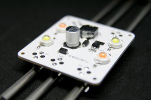
and labelled control module pane (right)
    First attempt at making the decorative front panes, the red LED pane is acceptable, but the control module pane was drilled incorrectly and ended up breaking

    14 of the red panes will be required to cover all of the LED positions, and a couple of customised panes for the power and control modules. As shown in the image, I had some trouble with aligning the drill to the target positions, and even managed to break the corner off the brightness module pane, requiring it to be remade entirely. In future I really should make a quick alignment guide and use a proper drill, rather than a small handle to manually twist the drill bits through.

    The LED panes are made from 2mm clear acrylic sheet with a stick-on red film tint to give the impression of coated glass. The film did make a mess around the screw holes where it was drilled through, though these will be concealed behind the panel anyway.

    The same 2mm acrylic is used for the control module panes, with printed paper labels simply stuck onto the back, and an additional central hole drilled out for the switch and potentiometer handles to protrude.

    I had also ordered a small metal potentiometer knob to hide the drill hole around the potentiometer shaft, but it turned out the shaft didn't stick out far enough from the panel to be able to fit it! Thankfully, one of my friends was able to 3D print me a replacement on short notice that I quickly modelled up in FreeCAD, as my own 3D printer is in dire need of calibration, should I actually get round to it...

    Small 3D printed potentiometer knob replacement
    I quickly modelled up this little potentiometer knob in FreeCAD and a friend was able to 3D print it for me the next day. Kudos!

    Due to the alignment error where I'd drilled the acrylic panes, I had to enlarge some of the mounting holes to allow for some play around the bolts. In hindsight, this is something I should have considered in the first place, rather than assuming near-perfect alignment between the panes and the panel cutouts. Still, after enlarging the drill holes and using a bit of force I was eventually able to get everything assembled:

    Fully assembled scanner bar
    Fully assembled with decorative front panes and potentiometer knob!

    Depending on the angle of the light, you can see where air bubbles have been trapped under the tint, and some specks of dust which got glued into the control panes, as I hadn't taken enough care to smooth out the film and keep the panes spotless. But overall, It looks reasonable and just needs a bit more time (and patience!) to do properly. I may end up redoing the panes if it bothers me, but it's good enough for now.

  • First light

    Eontronics08/09/2025 at 09:43 0 comments

    With all the functional components on hand and the PCBs finally assembled, I could now test the key point of whether the scanner actually worked. Being my first proper attempt at designing an almost entirely analogue circuit, I was expecting to have to spend a significant amount of time probing the boards with an oscilloscope trying to figure out why nothing worked. 

    So, I found a free micro-USB cable to power it all up and...

    First test of LED scanner bar
    First power up test of the scanner bar. I also tested off-camera the front potentiometer, for brightness adjustment, and rear trimmer potentiometer, for speed adjustment, with both acting more or less as intended.

    Success!

    While I haven't yet adjusted the sweep rate to the desired 1 sweep/second, the scanning behaviour works exactly as I had intended, and the fade-out of the LEDs gives a nice trailing effect, though I think it would be better if I made the fade-out a little bit slower. Still, I'm pleasantly surprised to see it all working on the first try, and there shouldn't be any significant roadblocks remaining to getting this all finished!

  • 3D printer spacers and LED enclosures

    Eontronics08/08/2025 at 14:31 0 comments

    At the same time as ordering the PCBs, I also used the opportunity to try out the 3D printing services that the fab offered. They seemed cheap enough and I needed the parts, so why not? Besides, their resin printers should give much nicer prints than my home FDM machine could!

    The first set of parts I modelled up were mechanical spacers for the power and control PCBs, to ensure the switch and potentiometer would be the correct distance from the panel when mounted to their PCBs.

    Control module spacer
    Spacer for the control module modelled in OpenSCAD
    Power module spacer
    Spacer for the power module modelled in OpenSCAD

    The spacers are both very similar in design, varying only in the central hole size and standoff height. They are quite simple in geometry, so lent themselves well to modelling in OpenSCAD. This was fortunate since I've stopped using Fusion 360, when Autodesk started to pay wall features behind their cloud-based "services" (In my case I had been using their linear finite element solver in a prior project and suddenly found I could no longer run models locally ):< ). 

    LED enclosure/spacer with parabolic "reflector" design
    Like the previous two spacers, the LED enclosure was also modelled in OpenSCAD, which was made a bit more interesting trying to generate the paraboloids to house the LED!

    The LED enclosure is a similar design but features a parabolic shaped "reflector" to surround the LED and hopefully provide a more even dispersion of light. As this is 3D printed, the light will of course be scattered rather than reflected, but it felt cooler to try and model a proper parabolic design in OpenSCAD rather than making it spherical.

    I had all 16 of the parts 3D printed in white SLA resin, which thankfully turned out pretty cheap thanks to how small they are, though I did have to pay for shipping twice since they were packaged separately from the PCBs at the time. 

    The layer lines on the finished parts suggested they were printed at a 45 degree slope from the print bed, however the resolution was fine enough that it's only noticeable up close, and still far better than what my FDM printer would manage!

  • Circuit boards!

    Eontronics08/07/2025 at 22:49 0 comments

    The module PCBs were ordered from the usual low-cost PCB supplier. To keep things as cheap as possible, The 14 LED, power, and control modules have all been amalgamated onto a single PCB which needs to be cut out and separated manually:

    Tiled PCB containing control, power, and 14x LED modules
    The modules were tiled as a single PCB for manufacture, with most surface-mount components assembled, leaving just one SOIC-14 chip and the through hole components to be soldered by hand.

    This is a 2 layer board with overall dimensions of 97x82mm, in order to qualify for the <=100x100mm discounts that several fabs offer.

    The power and control modules are designed to match the dimensions of XLR D-Series panel mount connectors used on the panel, while the LED modules are designed to fit across their diagonals:

    Mounting configuration of PCB modules on a 16x XLR 1U panel
    The power and control modules fit directly to cutouts at either end of the panel, while the 14 LED modules are installed across
    the diagonal of the cutouts. Background Image sourced from penn-elcom.com.

    The 8 way, 0.05" pitch through hole pads present on each module are to be used for inter-module wiring. Though only 7 signals are needed, I'd like to use ribbon cable to join the modules together more neatly, so the ground signal has been paralleled to an extra wire, as 8 way ribbon cable is far easier to find, making the extra wire available.

    However, trying to assemble these proved to be extremely tedious, even after getting help from my dad to do all the soldering! Using ribbon cable was apparently a terrible idea as it was awkward to line up with the through-holes, and the PVC jacket would keep curling back under the heat from soldering. Using individual PTFE coated wires was somewhat of an improvement, but the fine pitch meant bridging between connections occurred far too often, and was tedious to desolder and repair.

    In the end, I had to design another tiled set of PCBs to bridge between the modules, soldered directly to 0.05" pitch pin headers. This was more manageable, as the extra structure of the headers helped keep everything aligned and in-place during soldering, however this did double the number of solder joints required to 480 (!!!). Manual assembly labour required is definitely something I should put more thought into in future projects, because all that work is ridiculous.

    All 15 interconnect board tiled into 1 PCB
    I threw these interconnect boards together in a bit of a rush, so forgot to leave room for the bolts. Whoops!

    Even after all this, the interconnect PCBs still turned out to be somewhat of a hassle. The awkward shape made them difficult to cut out, and most of them had to be trimmed to some extent as I had forgotten to allow clearance for fixings on the LED modules. To top it all off, the cost of ordering and shipping the extra boards and pin headers likely entirely negated any savings from tiling the modules into a single PCB in the first place! 

    Clearly not one of my brightest ideas...

  • Control and Power Module Schematic Design

    Eontronics08/07/2025 at 11:05 0 comments

    In order to drive the LED modules to sweep back and forth, a control signal needs to be generated with a symmetric waveform, one where the "falling" half of the cycle is a mirror image of the "rising" half. Since each LED module triggers at a certain voltage according to its position in a resistor ladder, and each sweep traverses the bar at a constant speed, the voltage gradient for each half control signal should also be constant. From these requirements, the control signal should be the form of a triangular wave, which the control module should be designed to generate.

    Triangle wave generator schematic
    The triangle wave generator is almost a recreation of how a 555 timer works, but designed to allow the upper and lower thresholds to be defined externally

    The design I have come up with for the triangle wave generator is similar in concept to the operation of a 555 timer. U204A&B form a Set-Reset (SR) latch, the output of which determines whether a timing signal (the triangle wave output, in this case) is rising or falling. A pair of comparators compare the timing signal against an upper and lower threshold, and set/reset the latch to reverse the direction of the timing signal upon reaching the threshold level.

    U201B acts as a simple integrator to convert the high/low level output of the SR latch into a constant rising/falling gradient to make the triangle wave. The integration rate can be adjusted using RV201 to adjust the voltage gradient, and thus how quickly each threshold is reached, which sets the scan speed/frequency of the scanner bar. Since the feedback from the SR latch ensures the integrator stays within the upper/lower thresholds, there is no need for a resistor in parallel with C205 to mitigate DC bias.

    Threshold level setting schematic
    Threshold voltages set by the resistor network are buffered with opamps so they can also be used to drive the LED modules resistor ladder

    The upper and lower threshold levels are buffered from a simple resistor divider, giving upper and lower levels of 2.97V and 0.52V, respectively, from a nominal 5V supply. These have been buffered because the signals are also used to provide virtual power and ground levels for the LED modules resistor ladder, thus ensuring the triangle wave oscillates within the same voltage range as is across the ladder. The voltage levels are more or less arbitrary, and were chosen to provide as large a swing as possible, to minimise the influence of noise, while staying within the common-mode range of the LM358s (~2V below supply to ground) used in the control and LED modules.

    Brightness setting schematic
    Not much to see here - the potentiometers brightness signal is buffered by an opamp to provide a voltage signal that the LED modules can source current from

    The brightness control input to the LED modules is simply buffered from a potential divider network using a potentiometer to adjust the level. This can be adjusted between ~0V-1V, allowing the LED current to be set up to a maximum of 10mA (I normally find LEDs to be too bright so this is plenty more than enough for me), while staying wall withing the common mode range of the LM358, and the 2V limit from the LED modules design.

    As with the LED module, additional capacitance has been added to various signals to form RC networks for noise attenuation. These are probably not necessary, but they're a cheap addition for some peace of mind.

    Power module schematic
    The power module allows 5V to be supplied through choice of either a (flimsy) micro USB connector or a (much sturdier) barrel jack

    As I'm designing this to run directly from 5V, the power module is extremely simple. There are 2 power connectors, a micro USB and a barrel jack, and a switch (SW301) to select between them. SW302 is the front panel switch to turn the whole thing on or off, and it's more important that this one looks nice and has a satisfying tactile feeling more than anything. Besides, the current load of the entire device is fairly small anyway. C301 is an optional bulk capacitor which can be added to smooth out a noisy supply rail -...

    Read more »

  • LED Module Schematic Design

    Eontronics08/06/2025 at 18:43 0 comments

    The LED modules which form the scanner bar have two key responsibilities: Fading their LED on/off at a reasonable speed to approximate the look of incandescent bulbs; and to use the value of a shared control signal to determine when the scanning sequence reaches that module. 

    LED Module analogue control circuit
    Two operational amplifiers and a few transistors form the analogue logic needed to control the LED

    The LED is driven with a constant current feedback loop, controlled by U401B and Q402, which ensures the LED current is insensitive to its forward voltage. The instantaneous LED current is set by the voltage across C402, which is buffered across R407, corresponding to 10mA/V (minus the small base current to drive Q402). At 20mA, there is a 2V drop across C402 and hence R407. Adding a further 0.7Vbe requires U401B to source ~2.7V from its supply. As this is USB powered (say 4.75V minimum), this leaves 2.05V of headroom for the op-amp, which is about what jellybean LM358s can achieve.

    The network of C402, R403 and R404 are responsible for the fade control. When LED is increasing in brightness, and Q401 is conducting, C402 is charged from the level presented on the BRIGHT_CONTROL signal through an 18k resistor, and discharges much slower once Q401 is blocking, through a combined 138k resistance. This forms a low-pass filter with rising/falling time constants of 8.4ms and 65ms respectively. Used to control the LED current, this gives a very fast fade-in and a much slower fade-out, somewhat similar incandescent bulbs.

    U401A is used as a comparator, monitoring the position control signal to determine when to start fading the LED in. Another comparator would be needed to determine when the LED should start fading out, however as this corresponds with the next connected module fading-in, we can simply take that modules fade-in signal (labelled "position compare"), and feed it into a "strobe" signal, to disable Q401 by pulling its base to ground.

    Resistor ladder for determining relative location of LED module
    A simple resistor ladder provides a voltage level corresponding to the electrical position of the module within the scanner bar

    To determine the modules position in the scanner, and hence set the correct level at which it begins to fade-in, every module has a "dwell" resistor which, when serially connected, form a resistor ladder that outputs a voltage corresponding to the position of the module in the electrical series. Additionally, by changing the resistor value, we can increase or decrease its weighting in the ladder, allowing certain modules to stay "on" (dwell) for a longer portion of the sweep cycle. This is utilised in the two end positions, so the light appears to linger upon reaching either end of the bar, before returning back the opposite direction.

    Additional fast RC network are formed on the resistor ladder and "position_control" inputs to help attenuate noise that may be picked up in these signals, which span the full length of the scanner bar.

    Due to the limited output voltage of the LM358 and drop across Q401, the brightness control signal should be limited to ~2V, as there is a risk of clipping occuring beyond this. As this corresponds to an LED current of 20mA, there should be no reason to go any higher to avoid burning out the LED.

    In total, this means there are 7 signals that must be passed between each module:

    1. Power
    2. Ground
    3. Brightness control signal
    4. Position control signal
    5. Resistor ladder serial connection
    6. Resistor ladder return (this is a virtual ground reference for the end of the resistor ladder)
    7. Position compare/strobe signals

    Meaning each serially connected module would need 7 separate wires to connect it to the previous module, which should be manageable for the short module-module connections.

  • Concept

    Eontronics08/05/2025 at 18:04 0 comments

    I want to try make the appearance of the scanner bar as faithful to the actual design used on the car, and a key component of this would be to try and mimic the slow fade out effect of incandescent bulbs as the filament cools. In comparison, LEDs respond almost instantaneously, switching from light to dark as soon as the flow of electrons is stopped, so I would need to devise an analogue circuit to gradually reduce the LED current (and hence brightness) to recreate the same effect.

    I ended up finding a rack mount panel with stations for 16 XLR connectors, which I thought could be used as nice windows for the LEDs to shine through. With a power switch on one side and some kind of control on the other (speed or brightness), which leaves the middle 14 spaces for the scanner bar itself, demonstrated in the image below:

    Mock-up of scanner bar using 14 LEDs and control modules at each end
    Quick design mock-up of the planned scanner bar and controls. Background Image sourced from penn-elcom.com.

    Rather than trying to run wires from a control board to each LED individually, which could get messy quickly, I decided on making a "smart" (in an analogue sense) LED module which would be wired in series with other modules to create the bar. By designing the fade effect into each module, the number of wires between each module could be reduced to just power, ground and a "position" signal. The value of this position signal would determine which module should turn on, and the scanning effect could be created with a repeating signal that sweeps through each LED module. Such a signal would be generated through a separate control module in one of the end positions.

    While scheming the LED modules, It took some time to find red LEDs with a clear lens to use, as I thought that without the red tint they would look a bit closer to incandescent bulbs, though in practice I'm not sure if this would matter since they were going to be installed behind red plastic windows anyway. I also wanted to design some kind of reflector to house each LED and give a more uniform glow through each window, as opposed to a glaringly bright point source.

  • Motivation

    Eontronics08/04/2025 at 19:21 0 comments

    A while ago at work, some of my colleagues were discussing cool things to do with a shiny new server cabinet we'd received. Inevitably, one idea was to fill it with bright glowing LED strips, for example to have red flashing lights and sirens in the event of a nuclear meltdown failed build. And if your builds haven't failed (yet...) then it could do a cool animation while everything's still going smoothly. 

    The scanner bar seen on KITT from Knight Rider was an obvious contender for said cool animation with plenty of demos online running it on any cheap micro capable of driving similarly cheap addressable LEDs.

    Clearly, I must have decided that seemed too simple/easy, and as I'd been wanting to learn more of the analogue side to electronics, rather than relying on microcontrollers for everything. I decided I'd try to make my own personal version, using analogue circuitry wherever possible. 

    So, I found a nice looking server panel online (note: I don't actually have my own server rack to put it in), with cutouts for a whole bunch of XLR connectors and a low enough price tag, and got to work designing something to fit.

View all 10 project logs

Enjoy this project?

Share

Discussions

Similar Projects

Does this project spark your interest?

Become a member to follow this project and never miss any updates