-
Position Dot Window Circuit
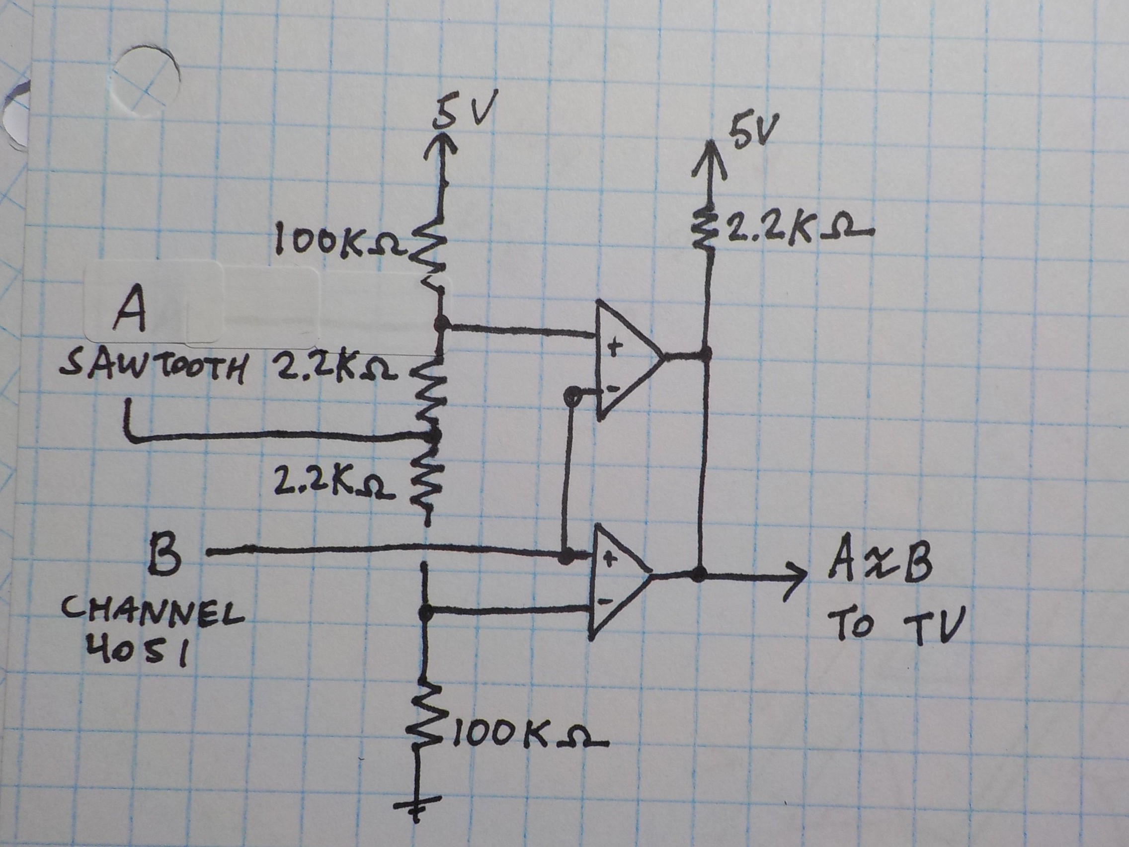
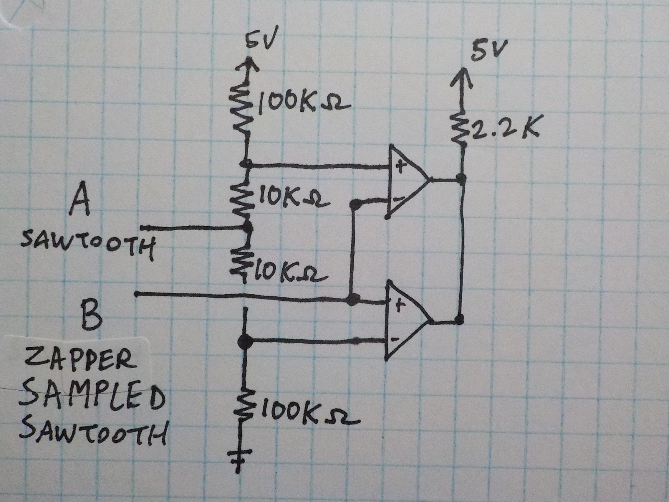
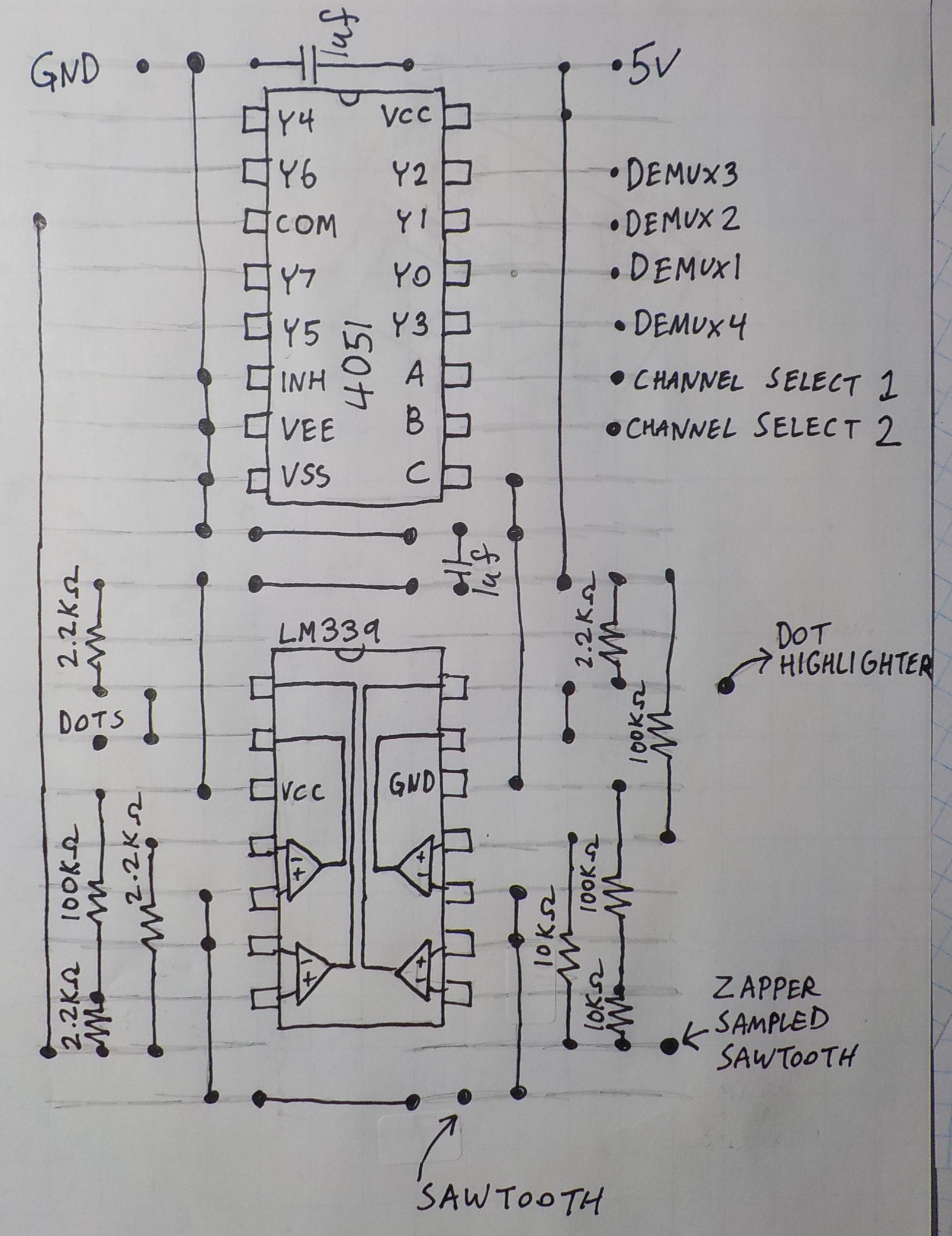
03/19/2017 at 20:53 • 0 commentsI need to display the voltages stored in the capacitors on the screen. I do this with a window circuit. A window circuit compares two analog voltages and outputs high only if they are a close match. If I compare the voltage stored in a capacitor to the sawtooth I will get a pulse when the rising sawtooth voltage comes to the same level as what's stored in a capacitor. The sawtooth rises as a scanline is drawn, so if this pulse goes back to the monitor it will produce a dot at a different point of the scanline depending on the capacitor voltage.
This same sawtooth wave was used to produce the values stored in the capacitors in the first place, so the positions of the dots will naturally line up to where the zapper was pointed when the capacitor voltage was set.
Textbooks typically show an AND gate or pair of diodes combining the outputs of a window circuit's comparators. LM339 has open collector outputs, meaning logic 1 is high impedance. This means an AND gate can be formed by connecting the outputs directly together and adding a single pullup resistor.
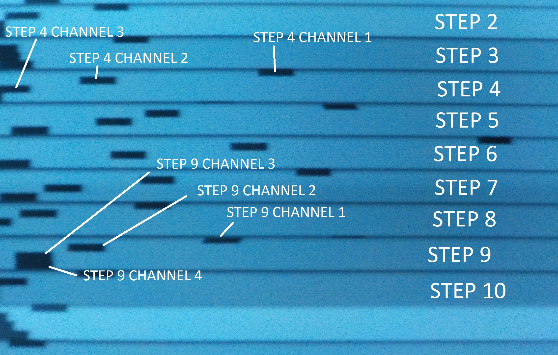
With each drum step I need to show dots for four control channels. I'm breaking each drum step line into four sections to show each of the channels. This is what the channel draw select bits are for. They cycle from 0-3 during the course of each count of the step draw. They control another 4051 demultiplexer which selects which of the four channels is being drawn.
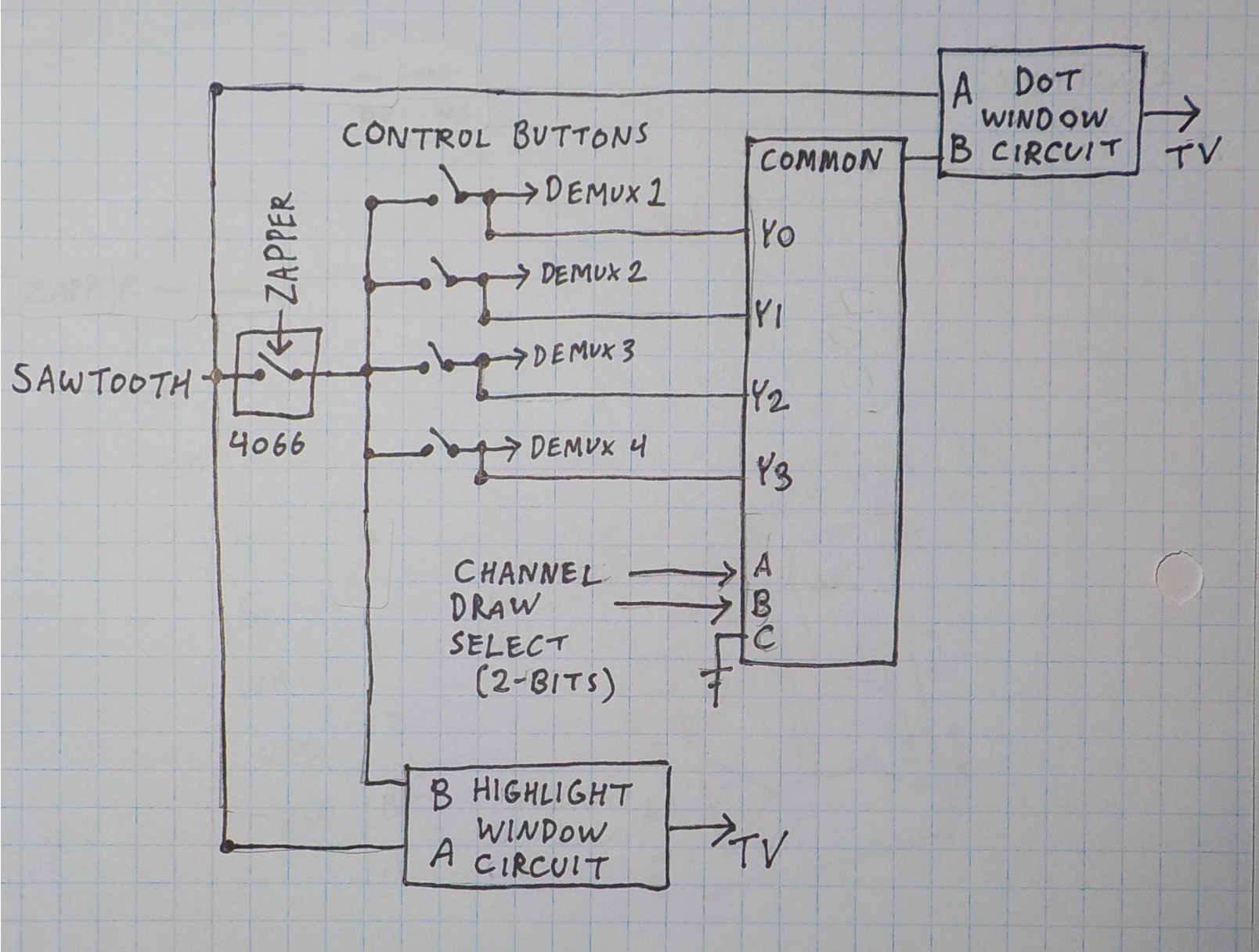
I was worried it would be confusing to look at the screen and figure out which dot belonged to which channel. LM339s have four comparators and I was only using two of them to built the first window circuit. I decided to use the second pair to form a window circuit that highlights the dots belonging to the control button being pressed. This was accomplished by connecting it between the zapper controlled 4066 and the row of control buttons. The voltage at this point is the output of the capacitor demultiplexer belonging to the control channel of the switch that's being held.
The highlight window circuit is identical to the first one except the 2.2kΩ resistors are replaced with 10kΩ for wider dots.
![]()
Channel one highlighting when control button one is pressed.
-
Analog Demux
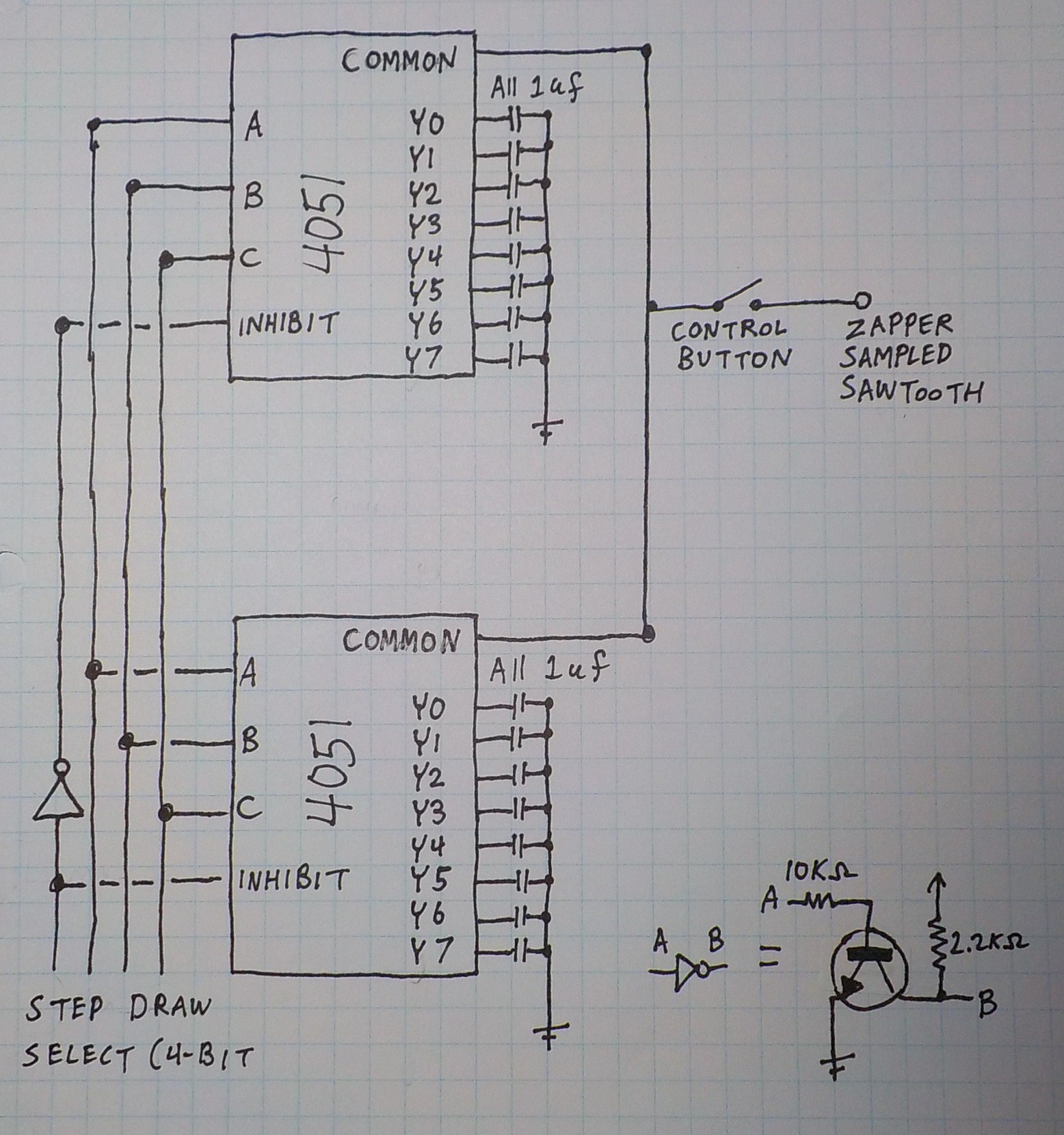
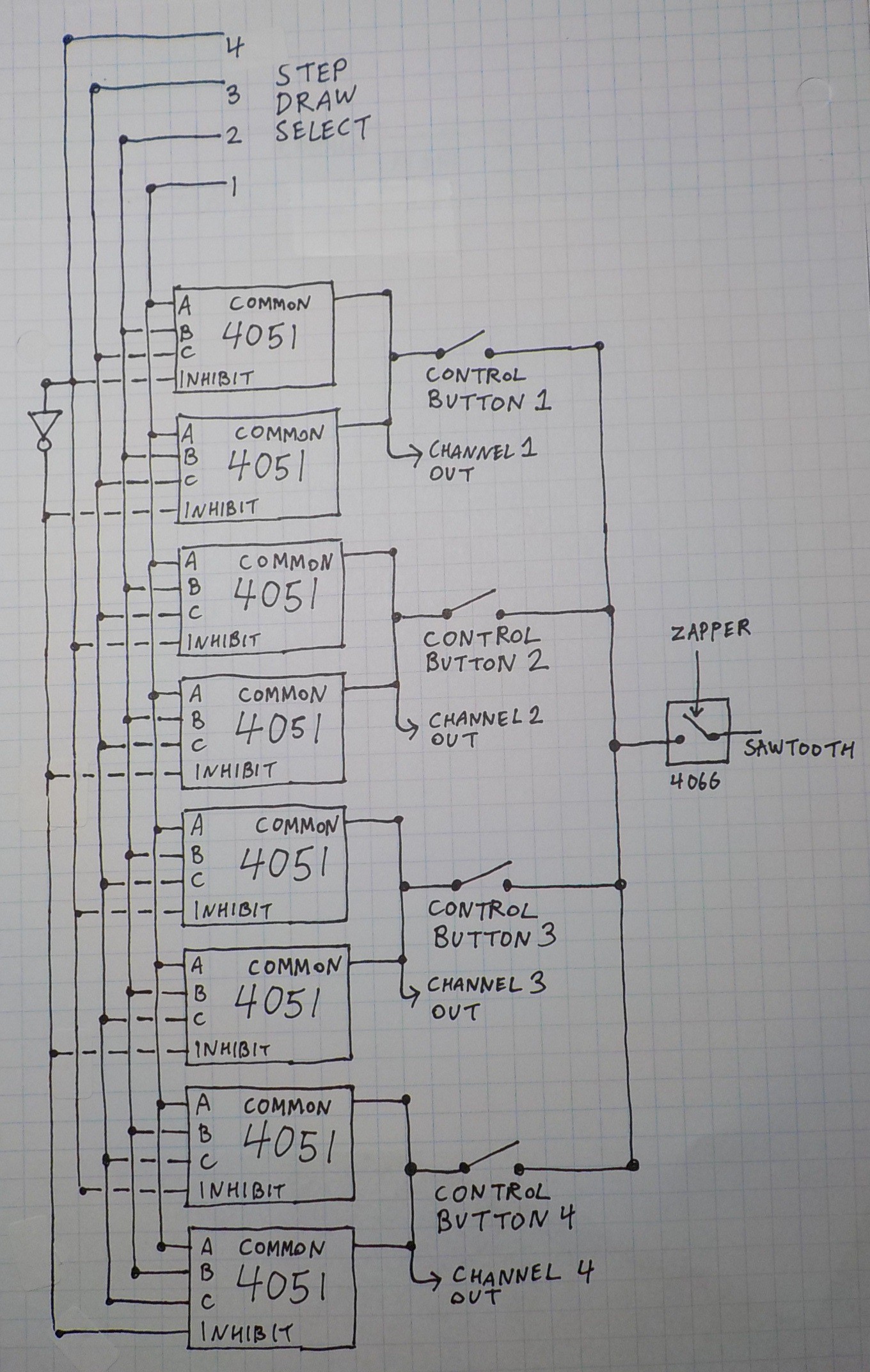
03/19/2017 at 20:00 • 0 commentsThis is the circuit used to store and access the horizontal positions of the dots. The position of the dots are stored as analog voltages in capacitors and accessed through 1-16 demultiplexers. There are four copies of this circuit. One for each of the four control channels.
Each circuit uses two CD4051 1-8 demultiplexers so there are eight in total for the four channels. CD4051s have an inhibit pin which is being taken advantage of to get two to work together to produce 1-16. With the inhibit pin active there is no connection between any of the capacitors and the common pin. A NOT gate makes the pair of 4051s alternate between which one is inhibited. Only one NOT gate is needed for the four channels because all four demultiplexers are always given the same address.
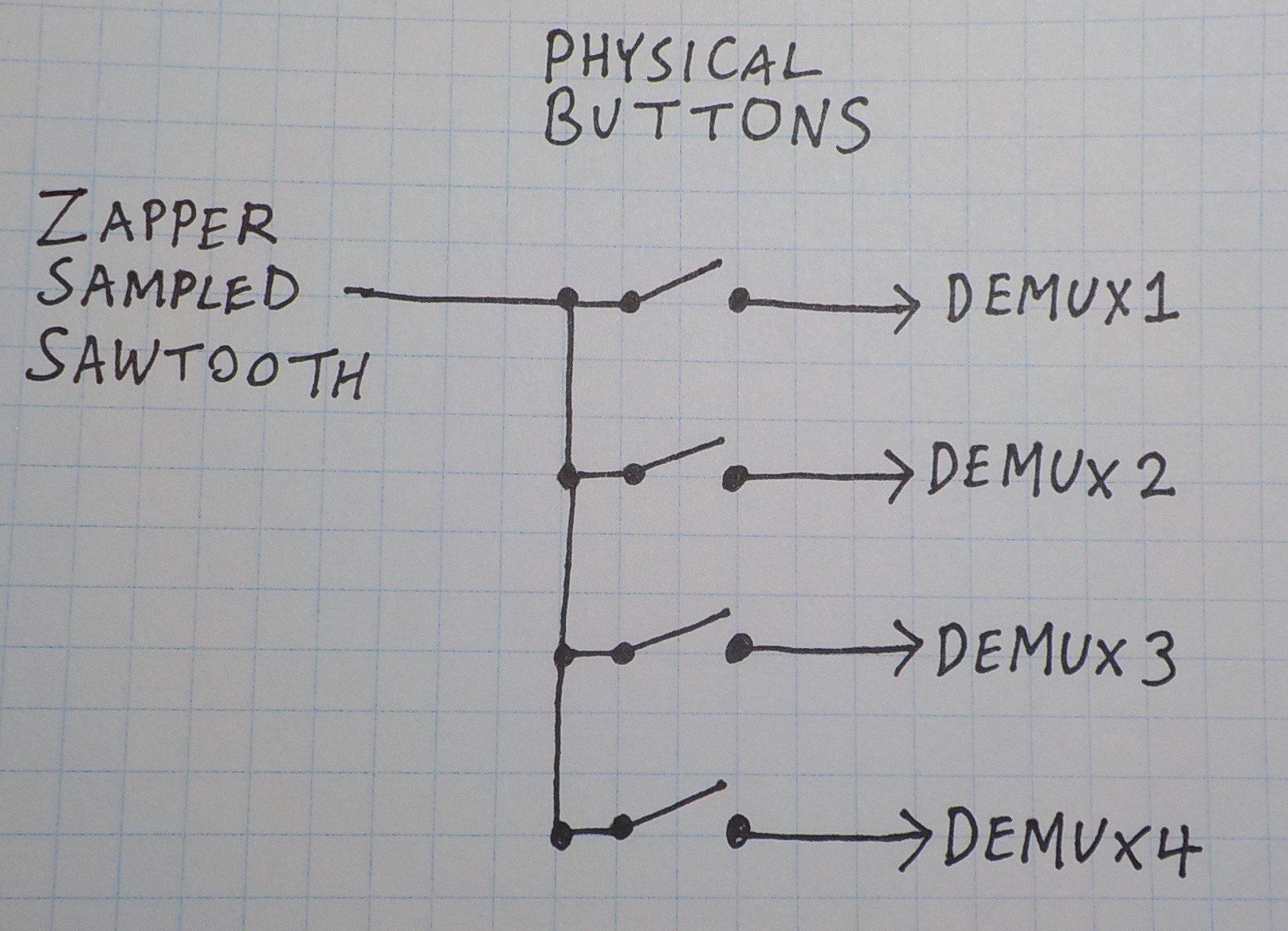
This diagram shows how all four demultiplexers are addressed in parallel and how the zapper sampled sawtooth is split through four physical buttons. Capacitors are not shown. Step draw select is the 4040 that counts from 0-15 as the screen is being drawn from top to bottom.
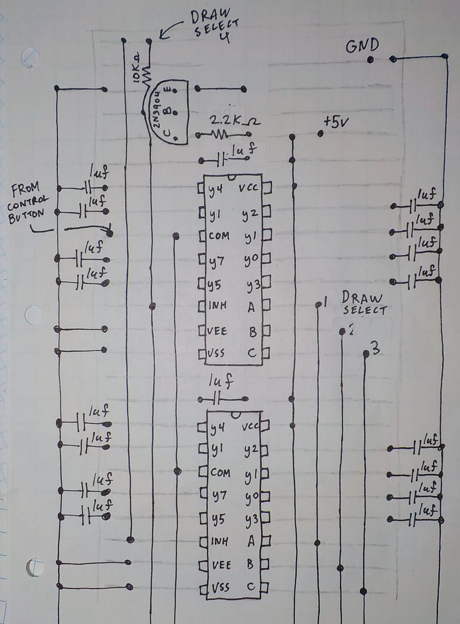
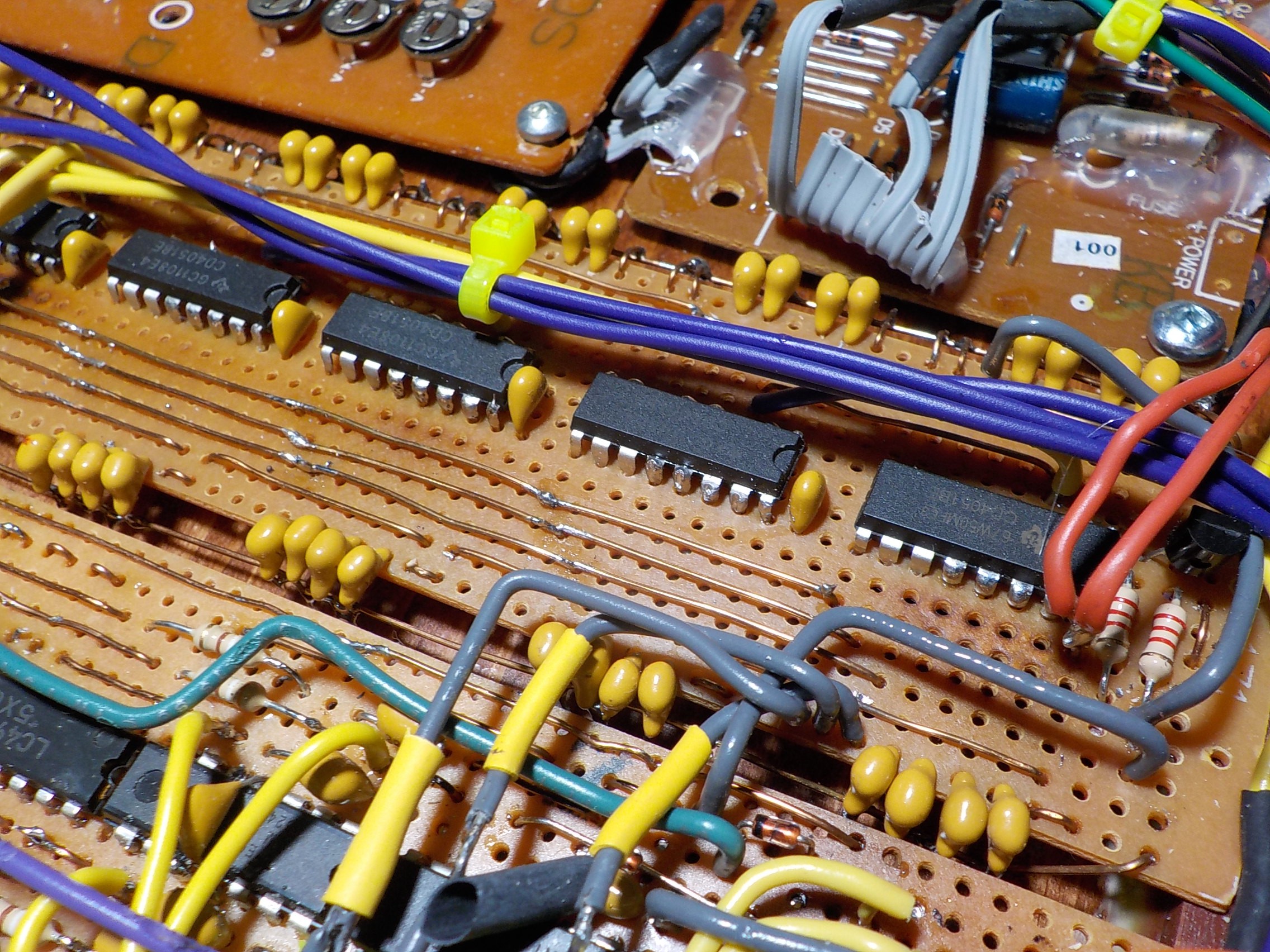
This is the stripboard layout showing the 2N3904 transistor use to produce the NOT gate for the fourth bit. Only two of the eight 4051s are shown. The placement of the 4051s is replicated three more times. The stripboards I used didn't have a power bus which was an issue for the large number of connections to ground required. I soldering a floating piece of bare copper to either side of the board to be the ground bus.
-
Control Buttons
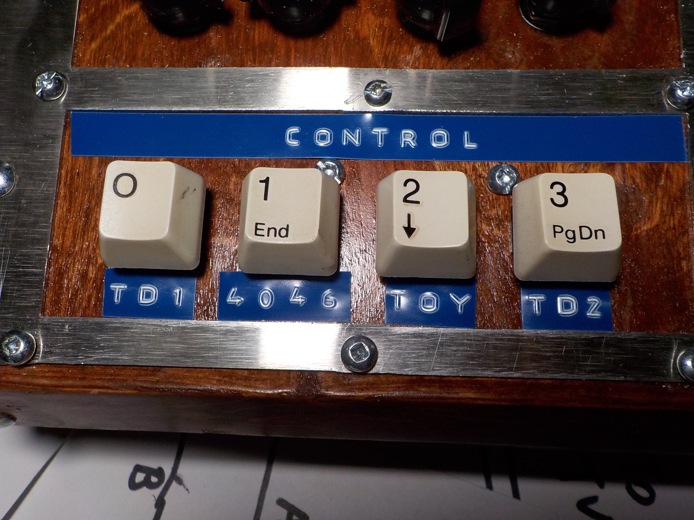
03/19/2017 at 03:31 • 0 commentsThis is the point where the signal chain splits into four separate elements for the four control channels. The output from the 4066 described in the previous step goes to four buttons. These buttons allow the analog voltage from the zapper sampled sawtooth to be sent to one of the four individual capacitor demultiplexers or none at all if no buttons are being pressed.
![]()
The buttons themselves are salvaged from an old keyboard. That keyboard was also the source of most of the wire and some of the resistors used for this project.
-
Sawtooth + Sampling
03/19/2017 at 03:16 • 0 commentsI need to create a sawtooth wave triggered by the NTSC Hsync. This can be used with a sample-and-hold circuit to produce an analog voltage that responds to the zapper's horizontal position.
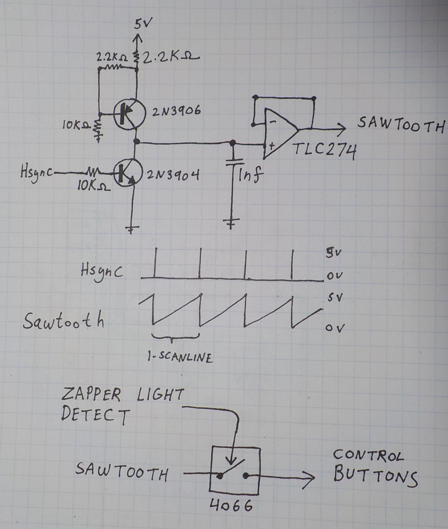
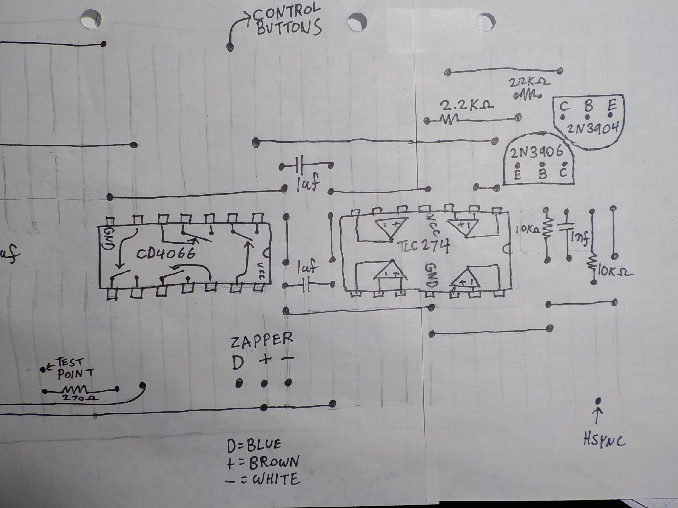
A 2N3904 is used to discharge a 1nF capacitor to ground at every Hsync pulse. The capacitor then charges up through a 2N3906 based current regulator. If the charge-up happened through just a resistor it would not be a linear sawtooth. The capacitor would charge quickly in the beginning then slow down at the end resulting in a rounded wave.
The TLC274 is used to buffer the sawtooth. Without it the voltage of the 1nF capacitor would be affected by the circuits recieving the sawtooth which would effect the waveform. TLC274 is a high speed quad op-amp. I only ended up using one of its elements, so I should have used a TLC271 single op-amp instead. That would have saved a dollar.
Audio op-amps like LM324 are not fast enough to handle the sawtooth wave properly. The buffer needs to be a high-speed op-amp.
The zapper light detection triggers a CD4066 switch to close. The input of the switch is the sawtooth. The other side of the 4066 switch goes a set of physical control buttons. (covered next)
A CD4066 has four switches in it, so this circuit uses the same chip that does NTSC video porching.
I cut open the Zapper's cable and soldered its wires directly to the breadboard. The detection wire is blue. Vcc is brown. Ground is white.
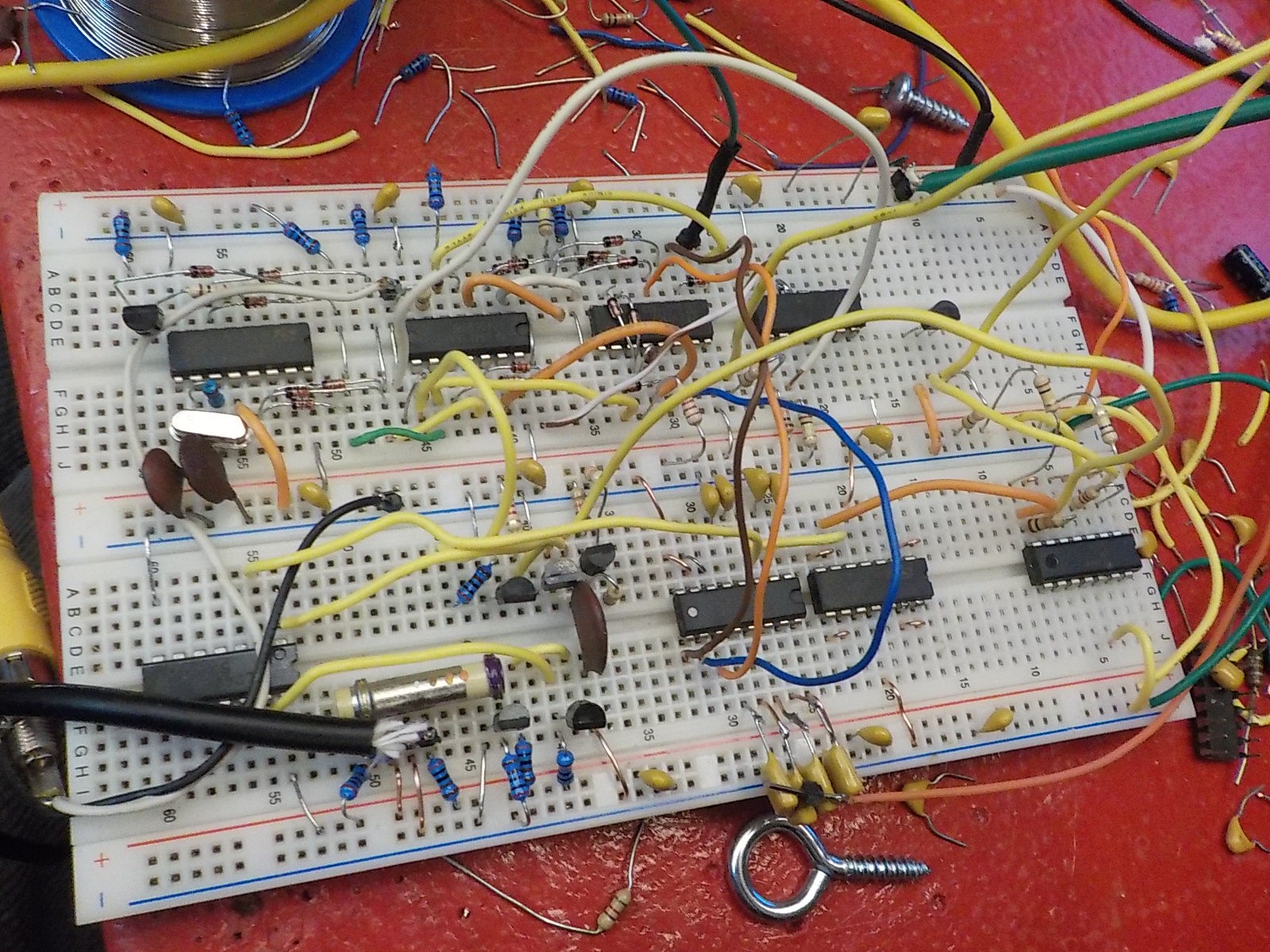
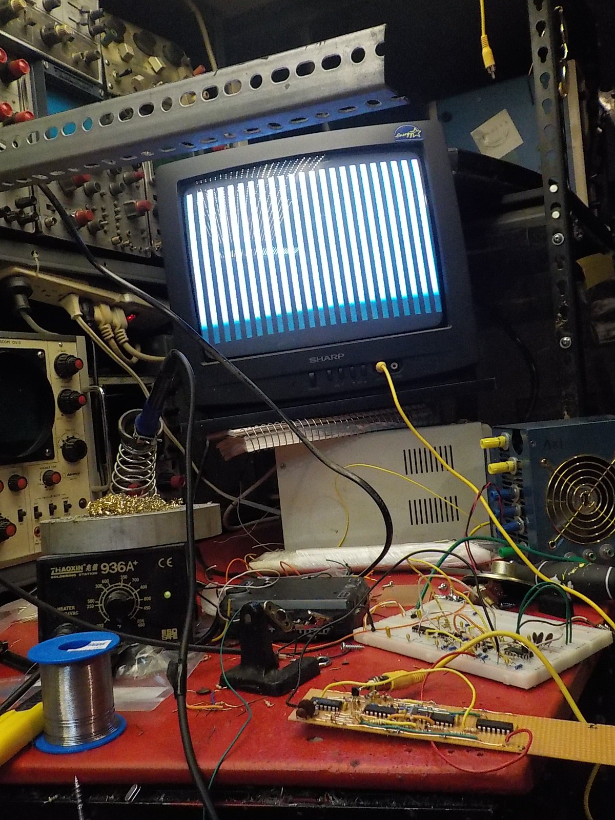
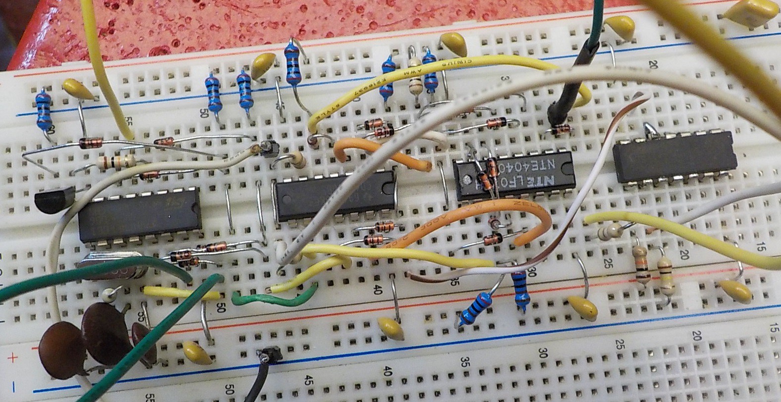
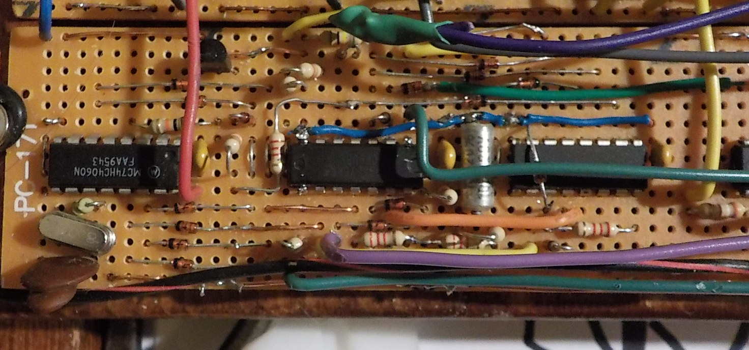
A look at the prototype so far. This is getting unintelligible so I'm going to stick to breadboard sketches mostly.
-
Zapper modifications
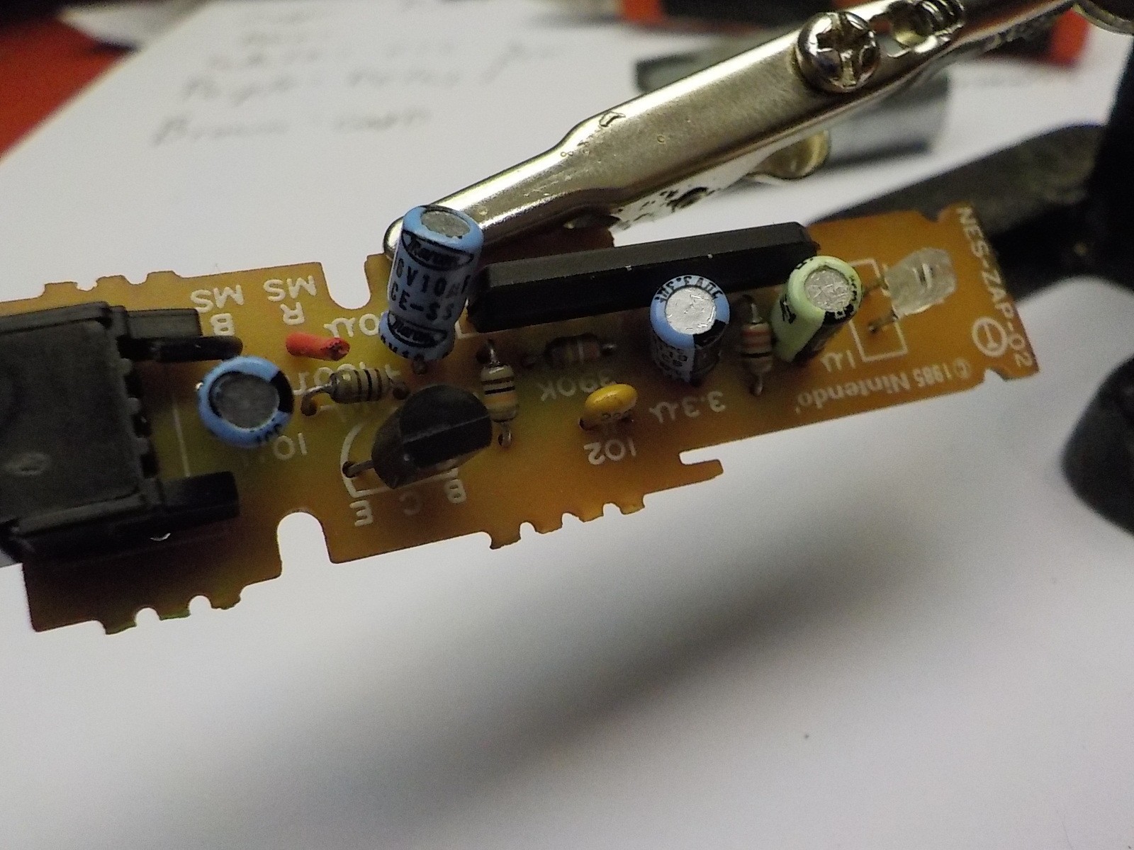
03/19/2017 at 01:21 • 1 commentWith older light guns like those used by Atari 2600 and Sega MasterSystem you could cheat at any game by simply aiming at a bright light. The game console flashes a white rectangle over a target then thinks the light gun was pointed at the target because it picked up light. Nintendo didn't want it to be that easy to see the last level of Duck Hunt, so they designed the zapper to not be fooled by this trick. It only responds to flashes lasting about a millisecond so it will not be fooled by a static light source.I opened up the light gun and took a look at the internal circuit board. Almost all the light detection work is done by an IR3T07A chip. I couldn't find a datasheets for this chip so I started poking around and trying to find a way to get the zapper to respond to static light sources instead of just flashes.
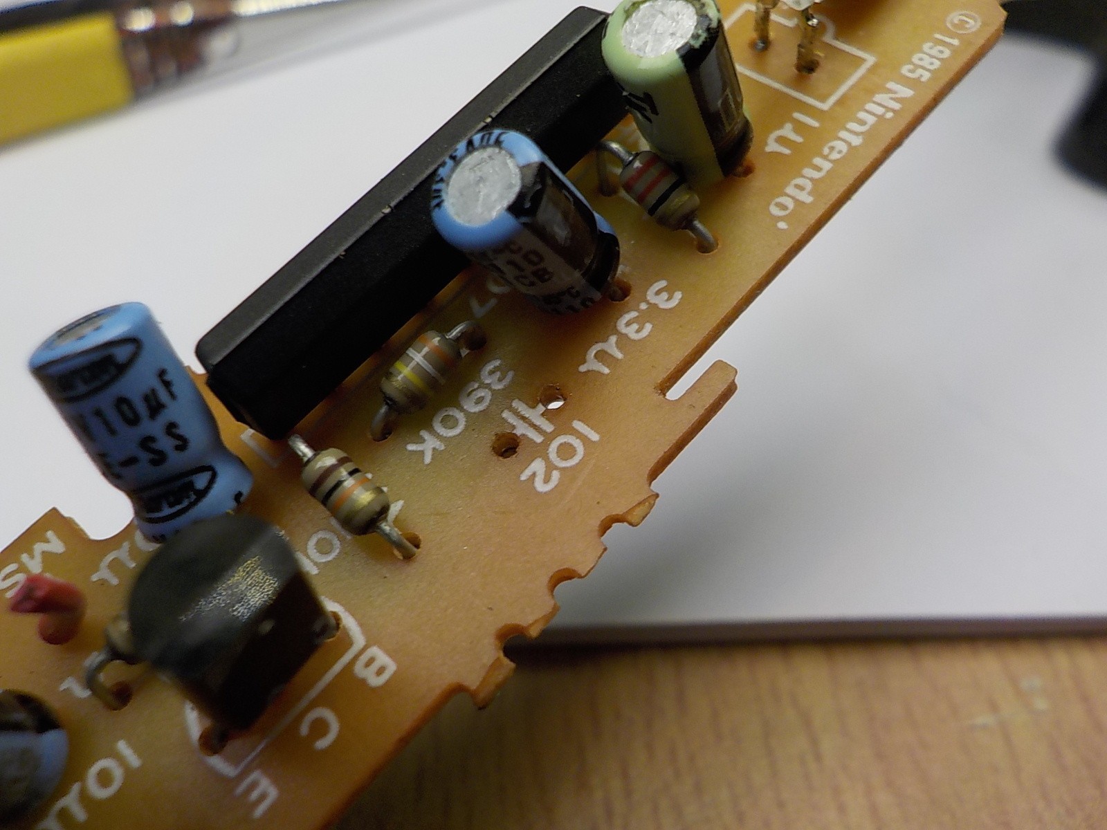
I eventually discovered I could get the results I wanted by removing the 10nF capacitor from the PCB. Strangely the light gun still doesn't respond to being pointed at a lightbulb, but it does respond to the CRT. I think the 10nF capacitor sets the acceptable light flash duration. Removing it leaves a couple pF between the PCB traces, which makes the invisible 60Hz flicker of a CRT acceptable, but not a static light source.
The transistor in the bottom left of these pictures is a BC458 (not to be confused with the common BC548).There was a random delay from 10-60 microseconds between the zapper seeing the raster beam and the signal rising on the detection wire; then again for the falling edge. This was a big problem for getting the horizontal position of the light gun. It was so bad the gun could appear to be on the opposite side of the screen because the detection pulse didn't activate until the next scanline started.
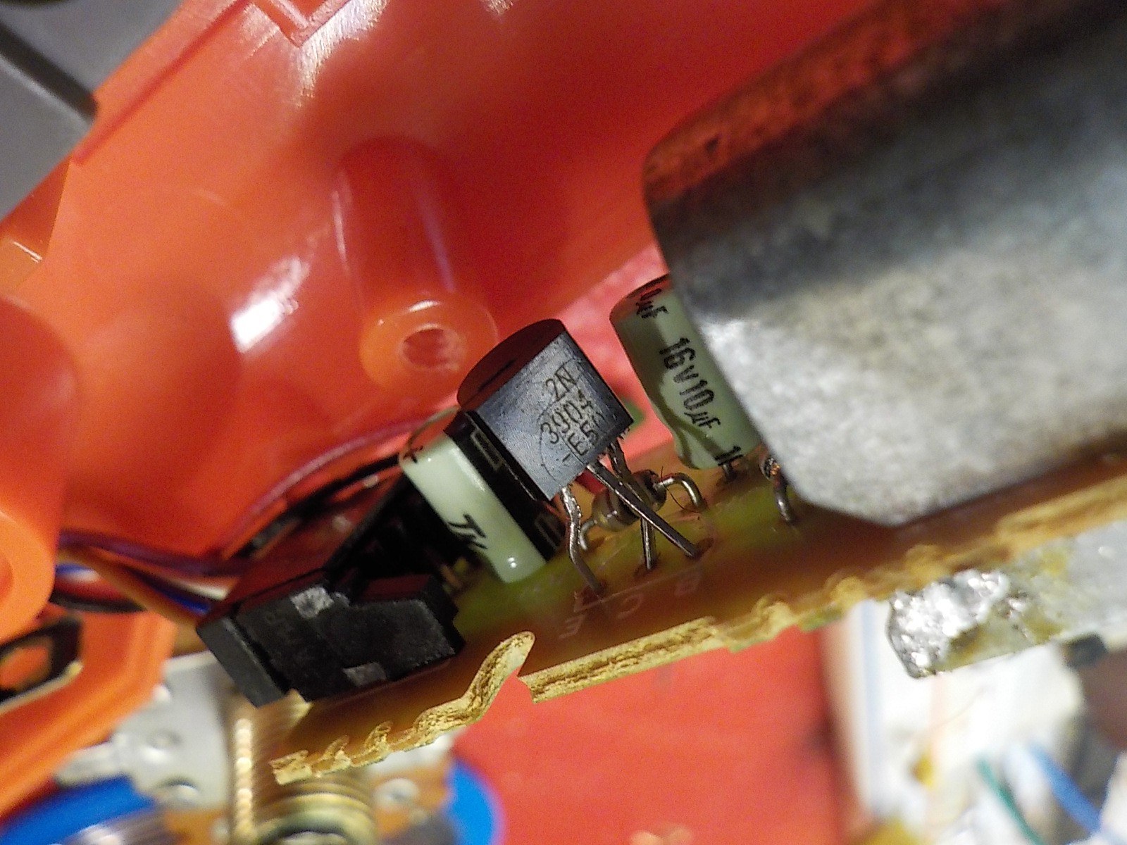
The Zapper uses the BC458 to boost the detection signal before it goes into the long wire. BC458 is one of the worst transistors the 80s had to offer and it's only gotten worse with age. A google search for it brings up mostly forum threads starting with "My X doesn't work" and ending with "Replacing the BC458 fixed it". I swapped it with a 2N3904 and it cleared up the problem completely. 2N3904 had a different pinout so there are bent leads to make it fit.
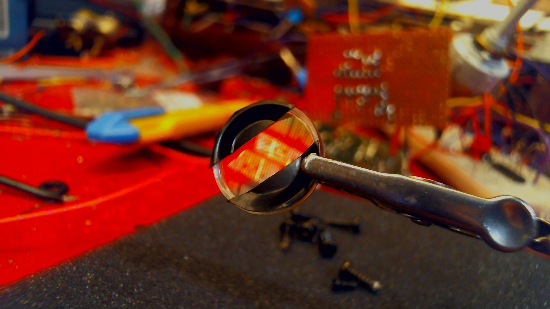
Later on I ran into a problem caused by the zapper's field of view being too large. Any of the drum sequence steps within the zapper's field of view will be moved when the control button is pressed. On a smaller TV the steps were smaller than the zapper's field of view so it wasn't possible to move one individually. Its neighbors would end up being moved as well. I solved this by narrowing the field of view with tape over the lense.
![]()
I also shortened the zapper's cable from 8 ft to 2 ft since it was unnecessarily long for my application and wanted to use the wire in other parts of the project.
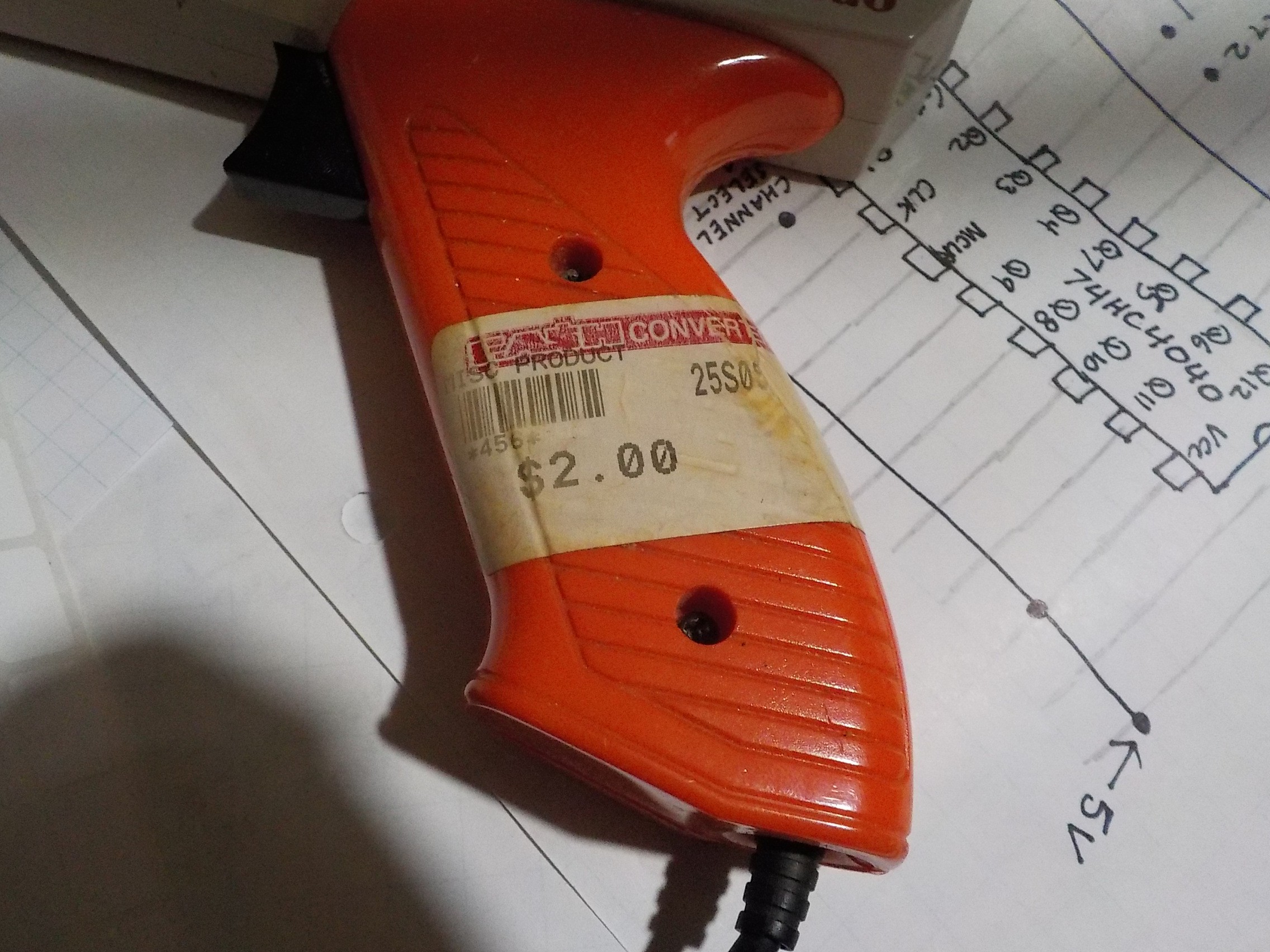
The zapper cost $2 Canadian dollars at a second hand store.
-
Display Line Counter
03/18/2017 at 20:05 • 0 commentsTouching the output pins of the 4040 binary counter will produce patterns of three lines, six lines, twelve lines and so on. There's a total of 240 visible lines in an NTSC video signal and the 4040 output pins provide that divided by powers of two. I want a total of 16 steps displayed on the TV and the closest I can get is 12.
I had originally planned to use the count from the 4060 which can produce 16 vertical lines, but this meant changing the demultiplexer state 260 times more frequently because it needed to cycle though all 16 positions once per scanline instead of ones per frame. This caused a lot of instability in the capacitor array.
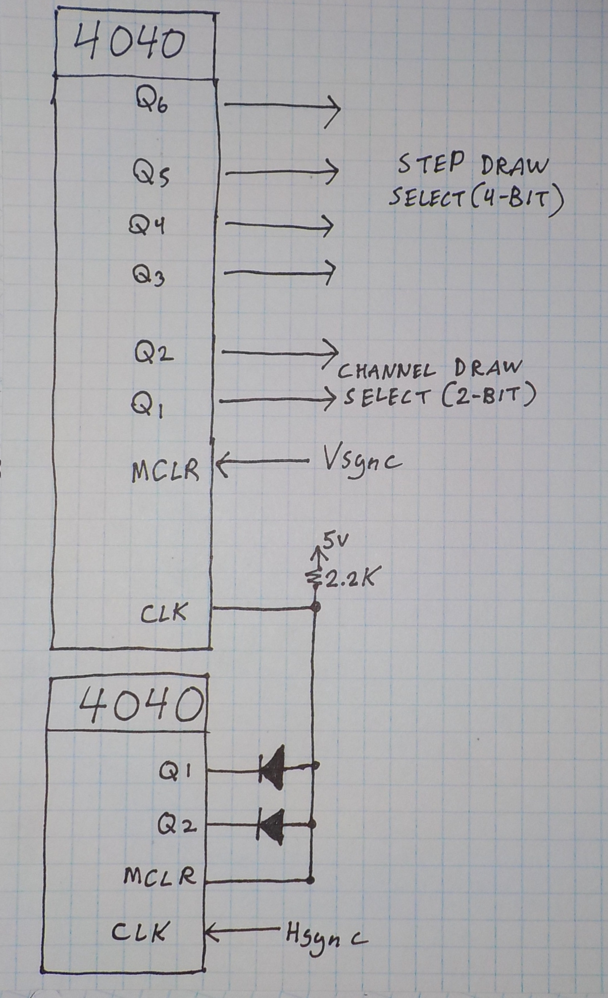
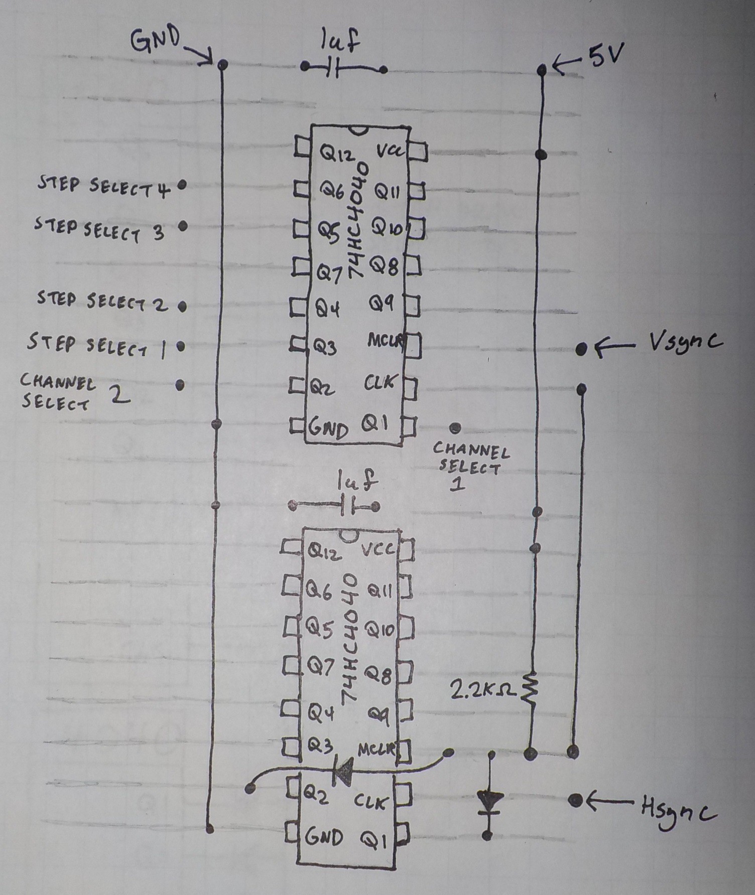
The solution is to add another set of 4040 counters. One for clock division of the Hsync pulse and one to produce a count going from 0-15 from that divided clock. There's another two lower bits which count from 0-3 for each step of the display draw count. These are used to draw the four channels in each step.
![]()
![]()
-
NTSC Signal generation
03/17/2017 at 04:45 • 0 commentsI need to generate an NTSC signal to give the TV. These contain the analog video combined with synchronization pulses and times when the video should be cut off known as porching. I decided to implement this with crystal oscillators and binary counters. I chose a crystal design because it's a lot more stable than Resistor-Capacitor or Capacitor-Inductor oscillators. A tiny amount of instability in a video signal is very noticeable to the human eye.
4060 is a binary counter with a built in oscillator driver. 4040 is a regular binary counter.
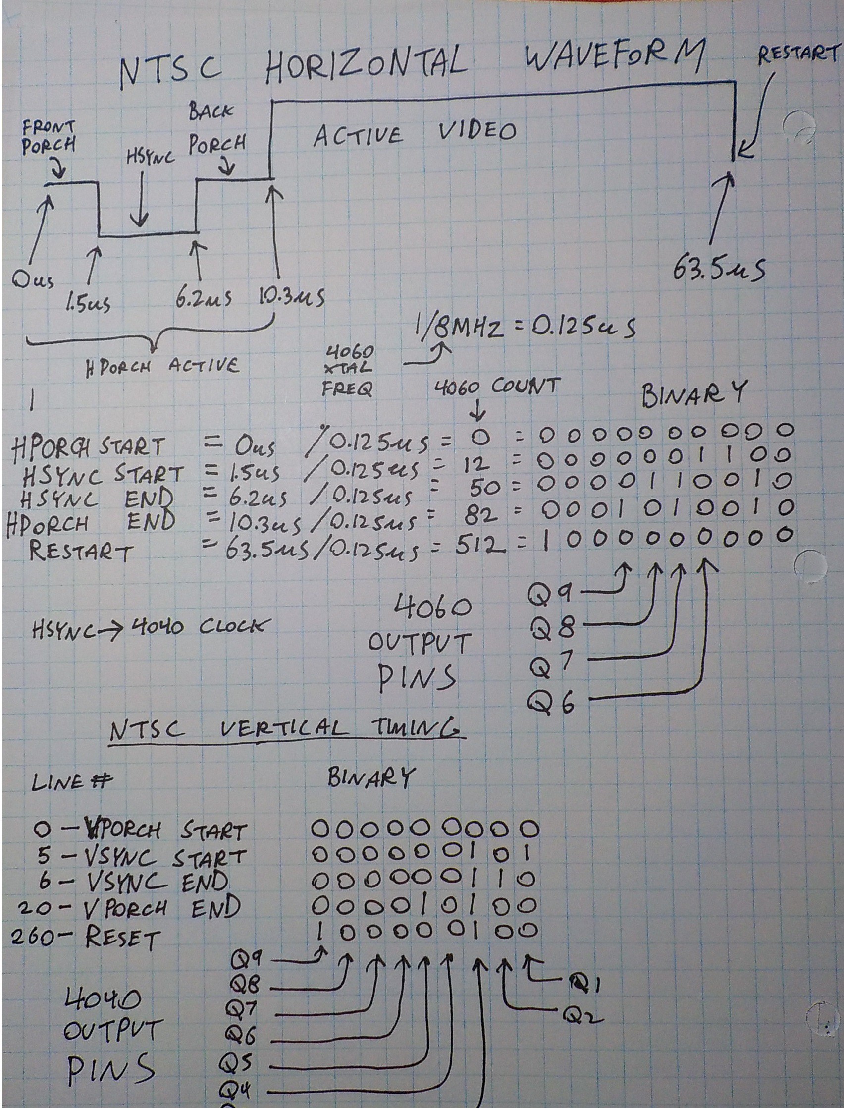
I got the NTSC timing information from this website and decided to use an 8MHz crystal. I ran the numbers with a several different common crystal frequencies and 8MHz required the least amount of logic attached to the binary counters.
My first task was to work out what the binary counter pins would output at the important stages of the NTSC waveform.
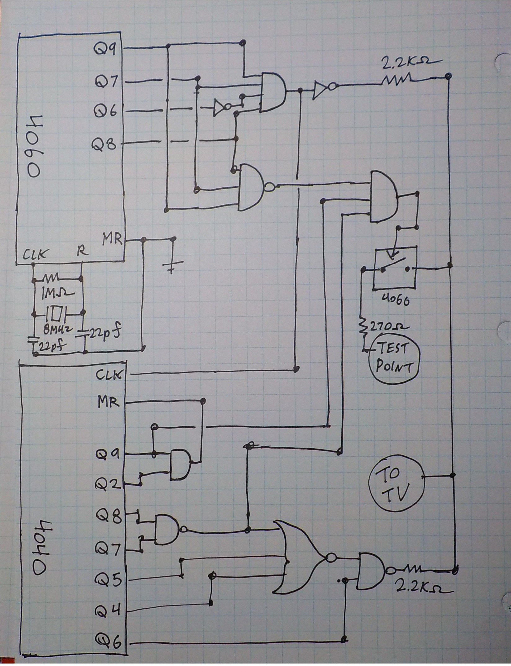
Next I came up with a logic diagram to get the porching and sync pulses to occur when they should. Porching is being accomplished by shutting off the signal through a CD4066 analog switch chip.
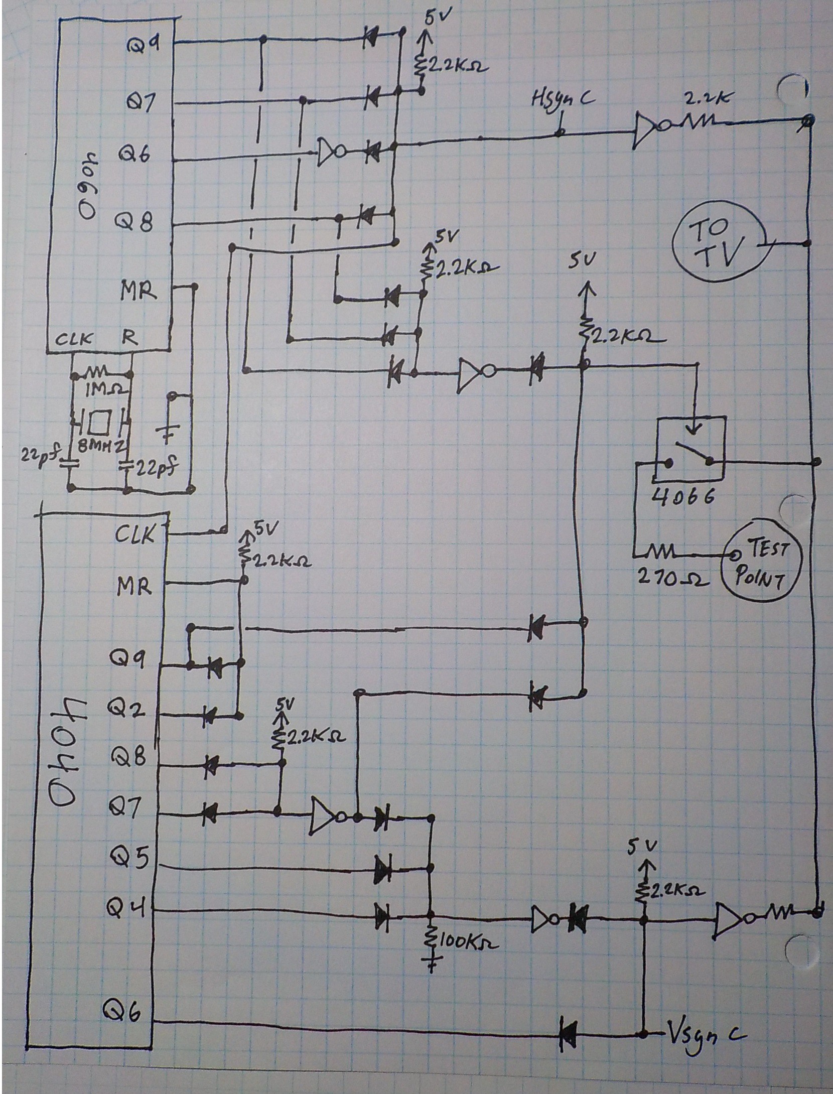
Next I convert the logic diagram to diode logic and inverters (NOT Gates). I like diode logic for projects like this because it makes everything a lot more inexpensive and compact. It would take three or four gate ICs and a spaghetti of wires to do the ANDs and ORs without diodes. It isn't possible to do inversions like NOT, NAND, NOR with diode logic. All diodes are 1N914.
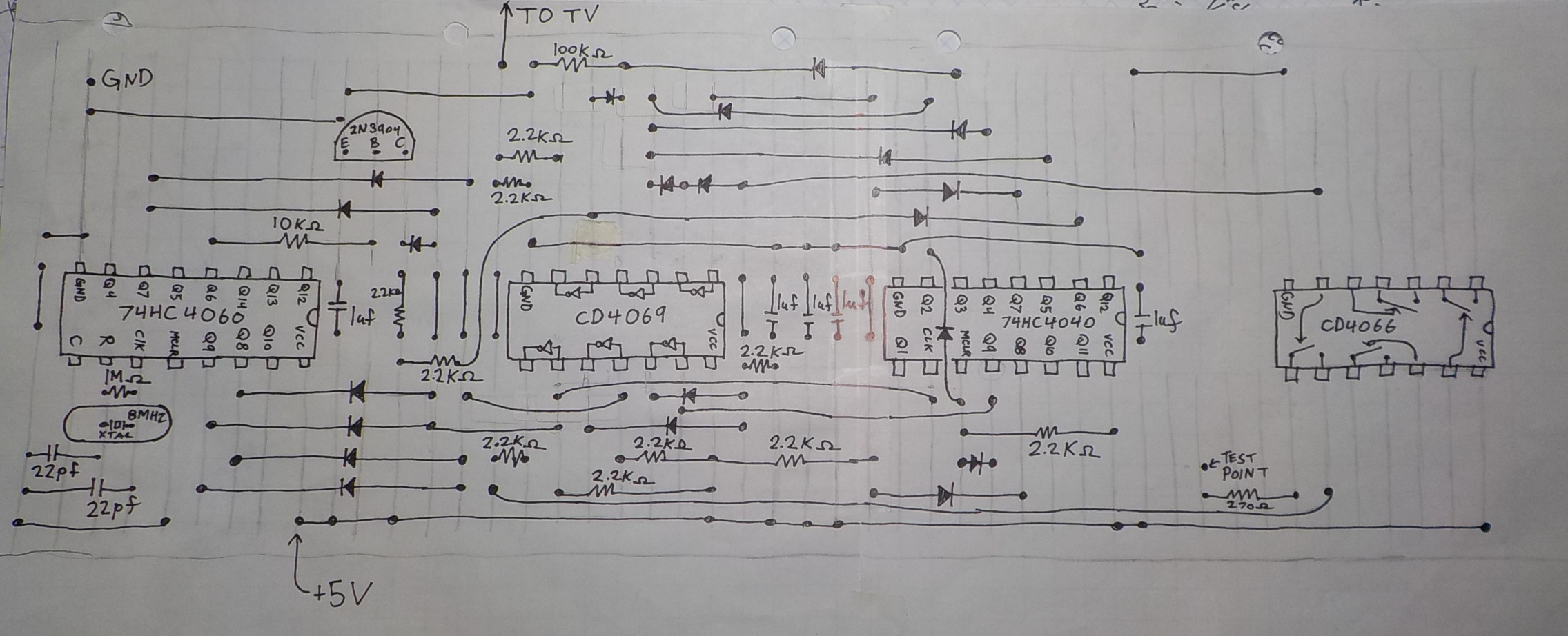
Finally I draw out a stripboard diagram. I'm using "Circuit Test PC-171" stripboards. They have the standard breadboard split down the center, but no power buses on the sides. In my breadboard designs none of the traces are ever cut.
The design called for seven inverters. I used a CD4069 which contains six inverters and a transistor inverter. I didn't want to add another chip just to get one more inverter.
![]()
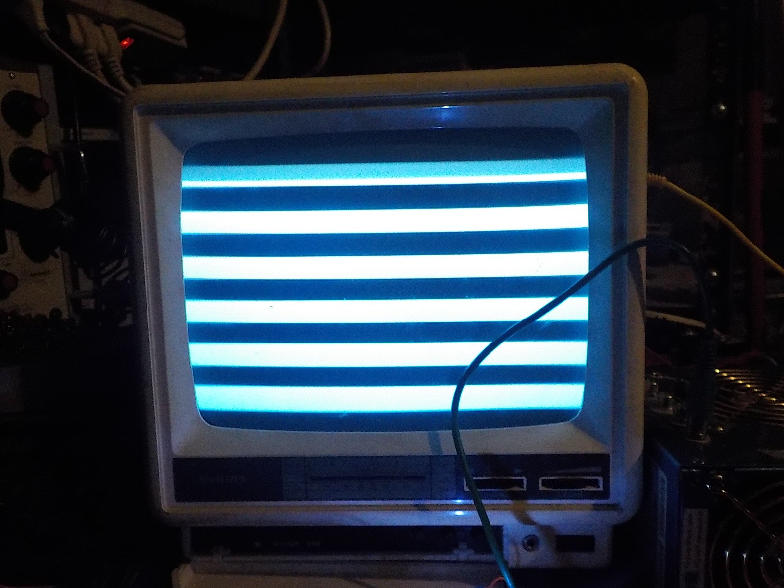
I tested it by connecting the test point to the binary counter outputs. Vertical lines from the 4060 and horizontal lines from the 4040.
These are some images of the prototype and final builds. There was still some fine tuning going on with the prototype so it doesn't exactly match the final design.
![]()
-
Power
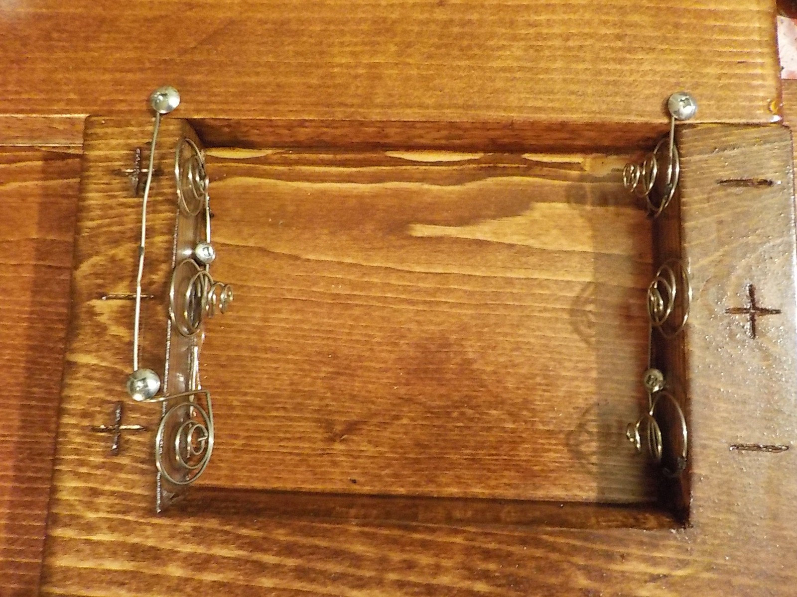
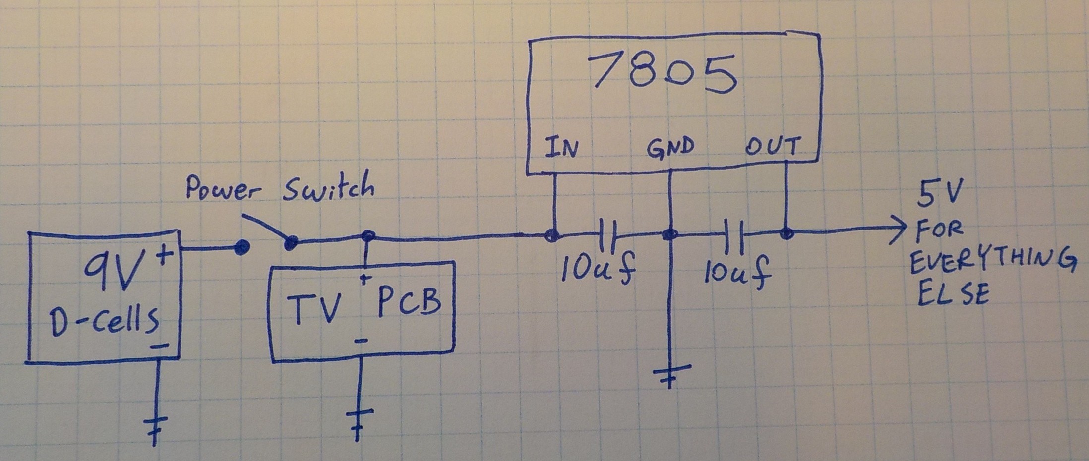
03/17/2017 at 04:06 • 0 commentsThe entire device is powered by six D cells (9v). The TV was designed to run at 12v, but does adequately at 9v. The screen becomes dimmer and the image shrinks to the center leaving more black edge space; but it's otherwise operational. I reused the springs from the TV's battery holder for a new one. + and - labeling was done with a hammer and flat head screwdriver.
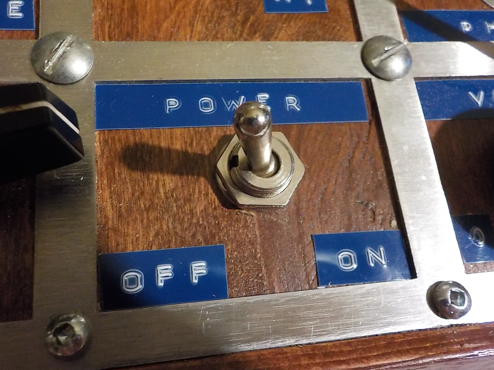
The TV's power switch was pretty crummy looking and I wanted to mount the TV PCB inside the case where it wouldn't be accessible. I desoldered the power switch and ran wires out to a panel mount toggle.
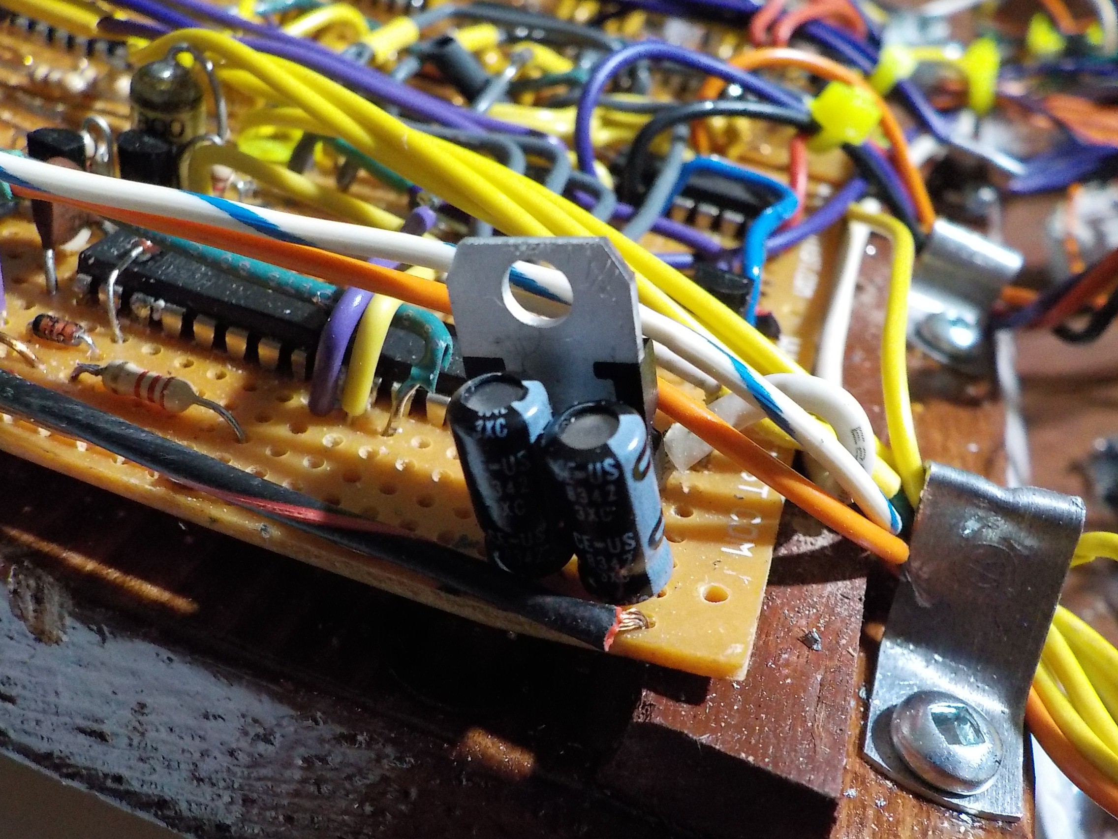
The NES Zapper and several other components were intended to run at 5v, so I added a 7805 (1.5A 5v Regulator). The regulator comes after the power switch. Everything except the TV is powered through the regulator.
-
CRT Television
03/17/2017 at 02:40 • 0 commentsThis project is built for the Moog Circuit Bending Challenge. The important rules are a budget of $70 and everything needs to be battery powered not exceeding 9v.
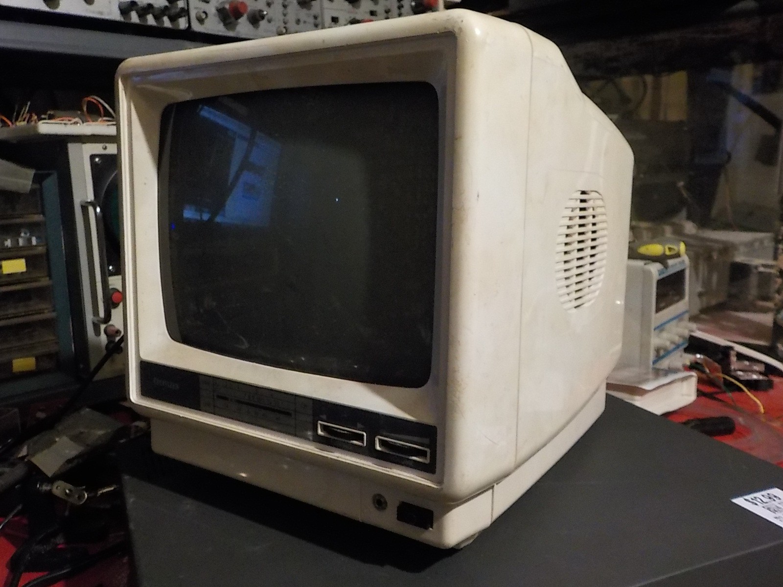
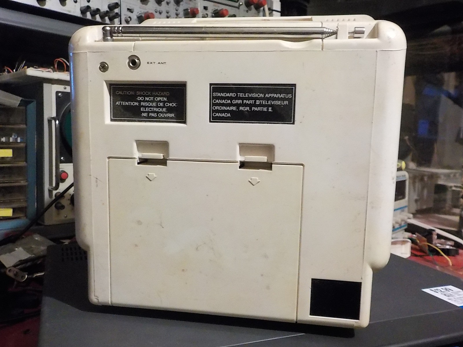
My circuits will work with any NTSC CRT television, but one that plugs into the wall would violate the 9v rule. I went to a flea market and was able to find a 19cm x 14cm Citizen Portable. I haggled it down to $5 CAD because it's black and white and doesn't work due to an issue I'll get to later.
This was a real stroke of luck since portable CRTs are almost always half that size. A larger screen makes using the light gun a lot easier. I spent the entire project terrified I'd crack the tube and be completely unable to find a replacement.
The issue with the TV: The only input source is an antenna. It has no coax or composite jack. The jack on the front is a 3.5mm headphone out. This TV has been a paperweight since analog broadcasts were shut down a few years ago.
I know North American analog TV broadcasts were NTSC modulated with an RF carrier wave, so inside the TV I should find an RF demodulator that outputs NTSC. The challenge is to figure out where that point is so I can cut out the demodulator and splice in a wired NTSC signal. I also want to take advantage of the TV's amplifier and speaker by adding an audio input.
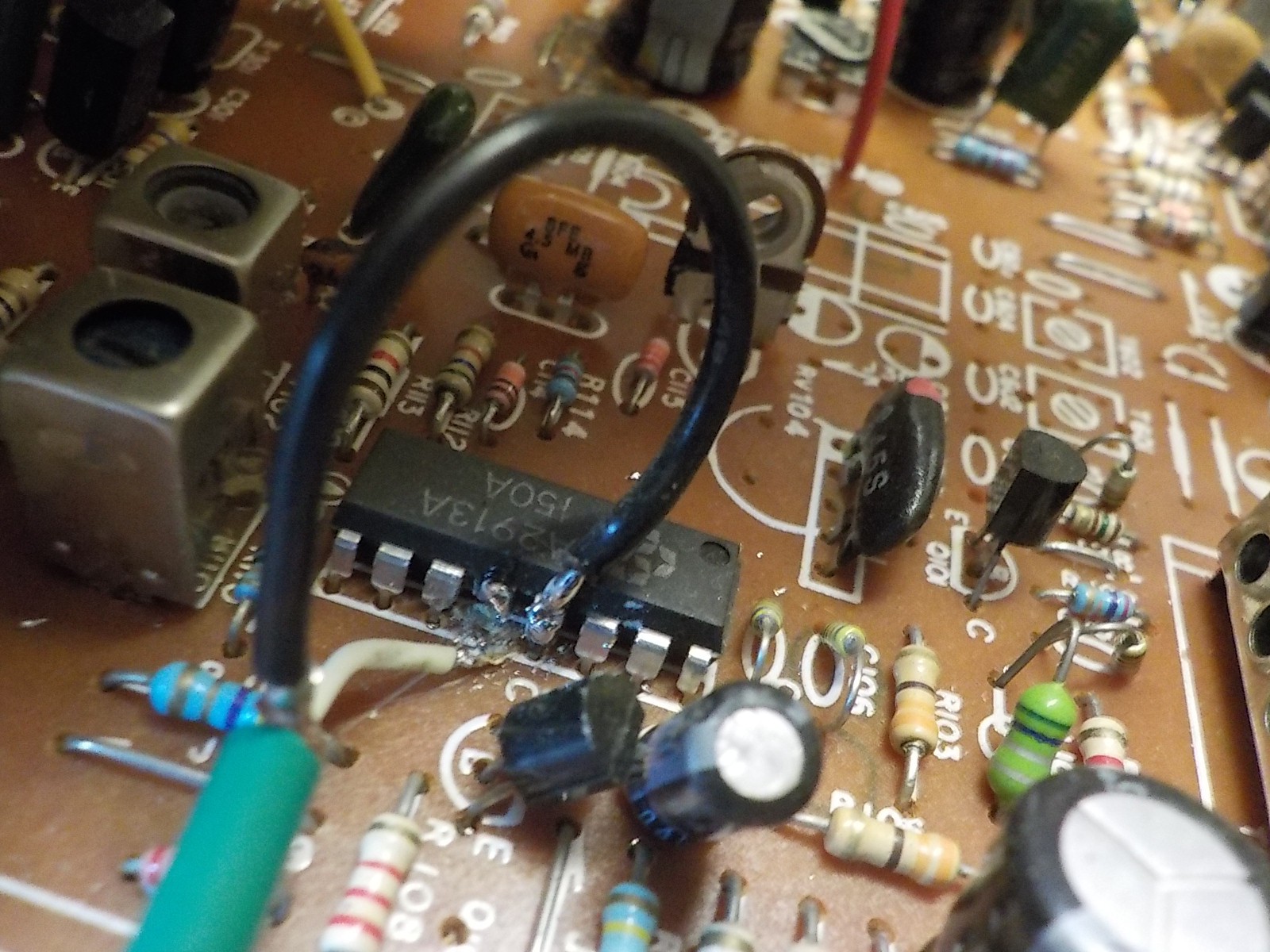
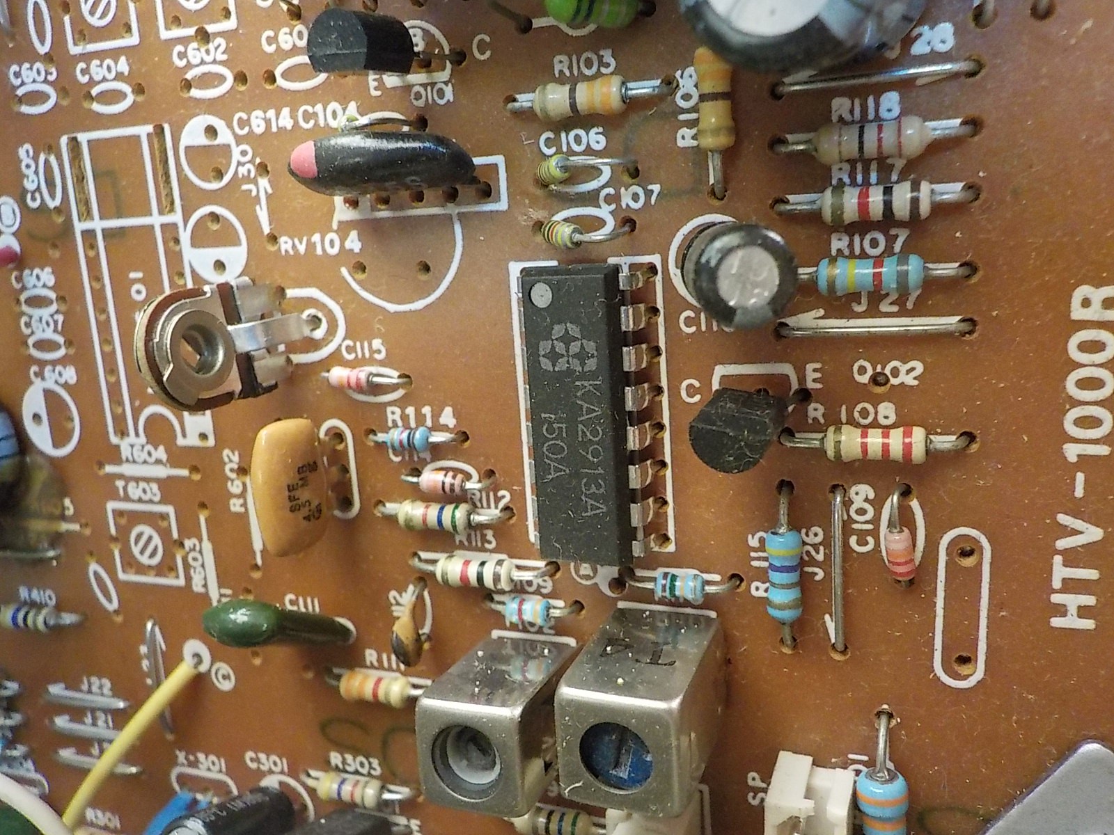
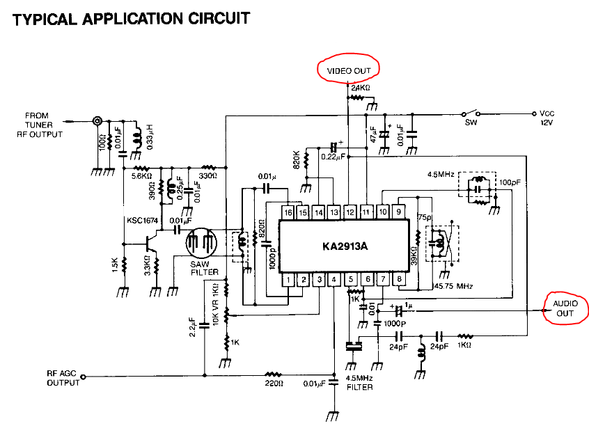
I looked at the PCB and saw variable inductors that were likely part of the antenna tuner. Above them is a KA2913A chip. A google search brought up a datasheet which told me this is a chip designed for TV demodulation and which pins contain the video and audio outputs. It's usually not this easy to get a datasheet for chips out of random electronics. My backup plan was to first identify the high voltage points on the PCB then poke the safe areas with the output from a VCR until I got an image.
I cut the chip leads then soldered a video wire to the pad. Ground needs to be connected too. Audio wire is not in this picture.
Now the TV can play a wired NTSC video signal. It's connected to a VCR in this picture.
![]()
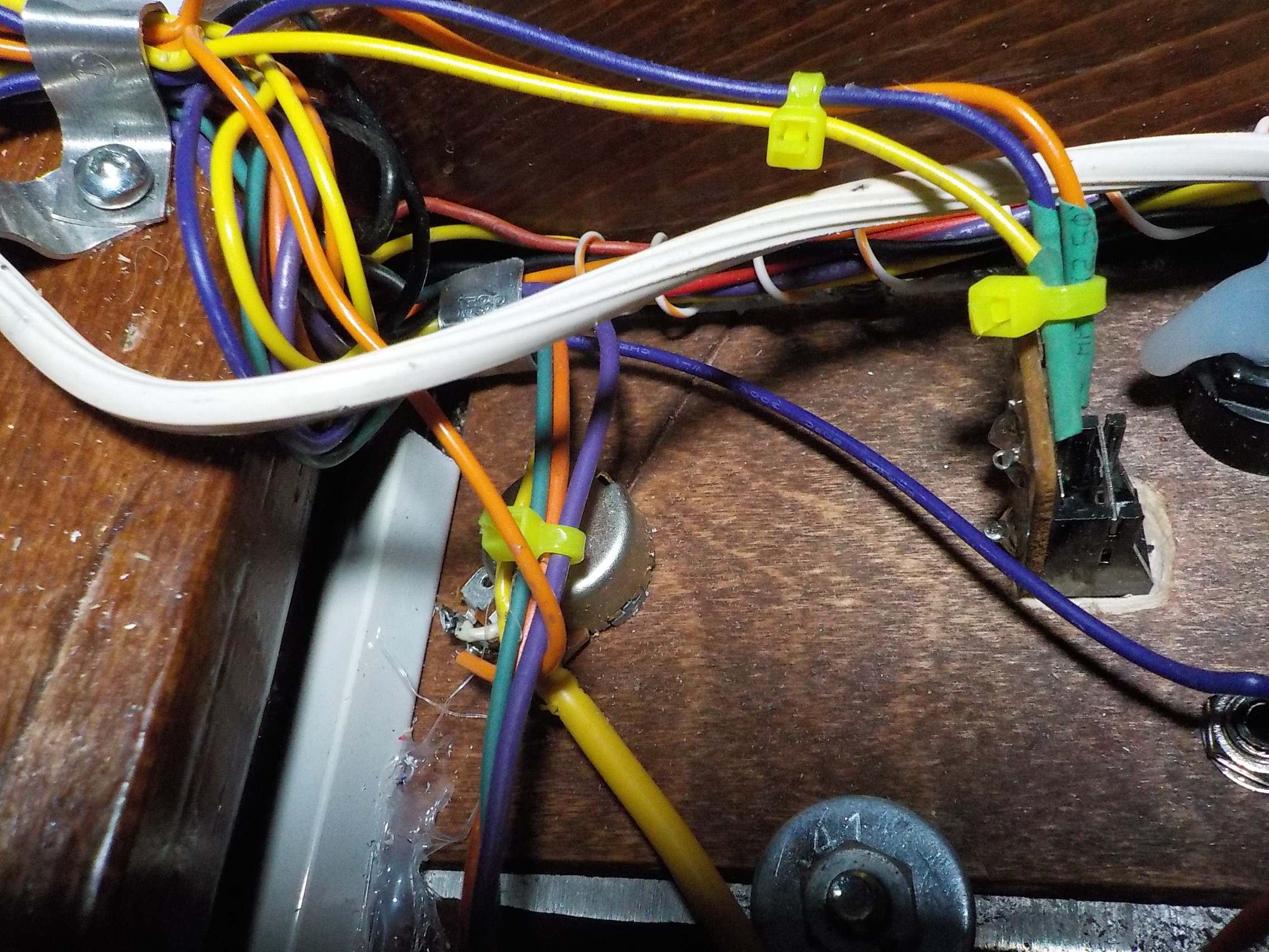
I found the demodulated audio point connected to the volume control potentiometer which was a much more convenient place to splice in a wire than the PCB. Creating an audio input to the TV lets me use the speaker, speaker driver, headphone jack, and volume potentiometer that were already part of it. The speaker sounded a lot better after being mounted to a wooden case.
Volume potentiometer on the left. Headphone jack on the right.
 Russell Kramer

 A CD4066 has four switches in it, so this circuit uses the same chip that does NTSC video porching.

 I cut the chip leads then soldered a video wire to the pad. Ground needs to be connected too. Audio wire is not in this picture.