 Cedric Honnet
Materials: For most FPCs, prototypes can be made from basic copper tape and Kapton tape. But when prototyping for high density designs such as our MCU PCB, the 40µm laser trace becomes noticeable vs the 150µm width of the MCU pads. In some cases, the laser might leave some microscopic metal hair, creating undesired electrical connections. Luckily, the accuracy of the results can be improved with a thinner copper layer. For example, some Dupont flex PCBs have a 9µm copper layer (vs 35µm in general). Otherwise a slow laser scan on the areas that need cuts can partially etch the copper layer and make it thinner.
Cutting VS Etching the traces: The laser can be used to either etch areas where there should be no conductivity, or to trace thin cuts around these areas. Since etching is slower than cutting along contours, solely lasing the contours can greatly accelerate prototyping. In our experience, this acceleration can go up to a factor of 10x, but it depends on the designs. However, only lasing the contours will increase the risk of short circuiting when the flexible PCB is bent, since the non-conductive separations are smaller.
Trace Resolution: The resolution or the circuit traces depends on the machine. Our best results were with the JPT fiber laser, achieving a 40µm cut and 40µm trace width, which is sufficient even for the MCU layout, our most challenging design. The lasing area has a size of 300mm x 300mm, which is bigger than any of our fiber modules. Our longest fibers measure 200mm, but as our MCU only measures 1.4mm, our entire MCU prototype board measured about 5mm x 5mm (see fig 22). Since this laser uses a Galvo system (Galvanometer), it also has a faster fabrication speed, i.e., our most complex fiber circuit takes about 5 seconds to fabricate on the JPT. Some prototyping illustrations:
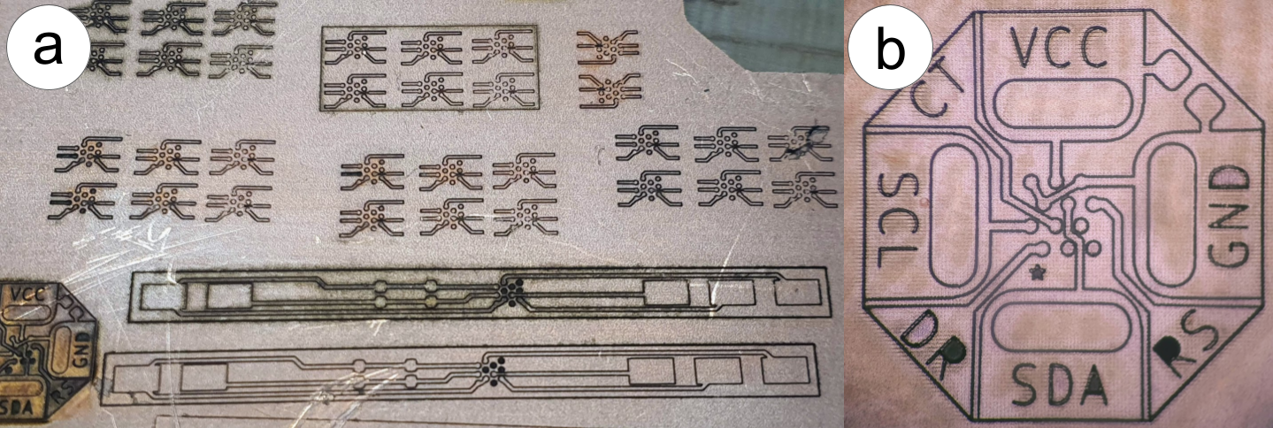
Lasing PCBs for quick prototyping, from 1st tests (a) to fully functional PCB ready to be assembled (b)
We also explored the use of a Trotec fiber laser which uses a CNC system with 1,000 ppi theoretical precision instead of a galvanic mirror. The best etching precision we obtained was about 120µm
trace width and 100µm cut width, which was sufficient to create our LED fiber modules, but not sufficient to create our most complex fiber designs, the MCU module. When attempting higher resolution cuts, we encountered PCB etching "hair" problems due to the limited software options available for the CNC control. However, the Trotec has a laser bed size of 300mm x 600mm, and could also be used to create flexible PCB boards for long fibers without the need to connect them.
Laser Cutting the Solder Mask: These lasers can also be used to create solder masks for the circuits, which avoid solder paste that may spread onto undesired areas. To create the solder mask, we applied masking tape to the top of the copper tape and etched it directly in situ. The solder pads image can be extracted from the gerber files of the PCB.
Laser Cutting Stencils: Stencils can also be made with these lasers, using the same file extraction method used for the solder mask. PCB stencils are not necessary if the used parts have solder balls, which is the case for our WLCSP parts (the MCU and the sensors).
Discussions
Become a Hackaday.io Member
Create an account to leave a comment. Already have an account? Log In.