 Alec Probst
Hi all,
This log will go through the calculations required to size the traces and vias for the StampPD PCB as well as the decision to move from a 2 layer board to a 4 layer board.
High Current Domains
We need to calculate what copper weights are required for the PCB based on the max expected current through traces and vias. For StampPD, we have 4 power domains that have significant current. These are:
- USB PD VBUS domain: 5A
- Determined by USB PD spec
- 3.3V Output domain: 2A
- Determined by buck converter max output current
- 5.0V Output domain: 2A
- Determined by buck converter max output current, and
- Input current to combined 3.3V and 5.0V buck converters: 4A
- See calculation below
Buck Converter Input Current Calculation
While the buck converters for 3.3V an 5.0V can output up to 2A of current each, they require a different amount of input current. To calculate each buck converters input current, we multiply its Max Output Voltage by the Max Output Current then divide that by the Minimum Input Voltage times the Efficiency.
The minimum Input Voltage for both buck converters will be 5V as this is the minimum voltage defined by USB. The efficiency can be found in graphs for the AP63200 but no 5.0V input voltage line is given. For now I'm taking the 12V input voltage efficiency at 2A which is around 90% for both buck converters. The actual efficiency is likely higher than this as efficiency in a buck converter increases as the input and output voltages are closer in value. By replacing the equation values and adding both buck converters input current requirements together, we get the below solution:
This gives us 3.7A which I round up to 4A for safety margin.
Trace Width Calculations
KiCAD has built-in "Track Width" and "Via Size" calculators that I'll show here. To start with, lets look at the 5A domain with default 1oz copper weight at 10C temperature rise for around 30mm conductor length ( length doesn't change track width much here so we'll default to 30mm since this is the length of the PCB ).
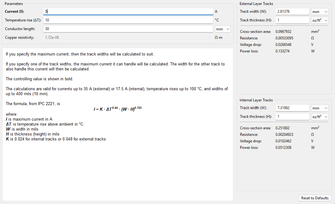
This gives us a 2.81mm trace width for external layers. For a 30mm x 30mm board, this is huge! This trace alone will take 1/10th of our board space in a single axis at a minimum! Reviewing the data sheets for all IC's, we can increase the temperature rise to 20C safely for all of our components with minimal loss in efficiency to get a trace width of 1.85mm. This is still quite large and doesn't provide enough routing flexibility. This leaves one last thing to change which is the Track Thickness, also known as Copper Weight. By changing this from 1 oz/ft^2 to 2 oz/ft^2, we get a track width of 0.92mm.
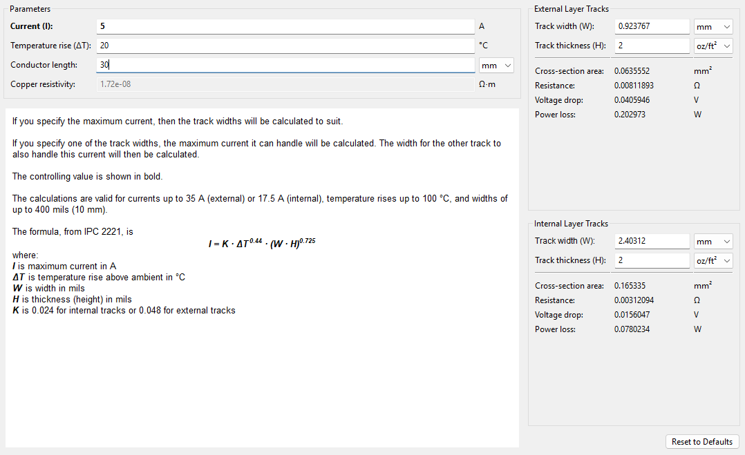
Rounding this trace width up to 1mm gives us a bit of a safety margin and is easier to keep track of. Increasing our Copper Weight to 2 oz/ft^2 will increase the price of the PCB but there isn't much choice if we want to support 5A. Note that a 1mm wide trace width for 5A is only valid for PCB layers that are external ( top and bottom layers ). Internal layers will need much thicker traces as they usually have lower Copper Weight, usually 0.5 oz/ft^2, and can't remove heat as easily.
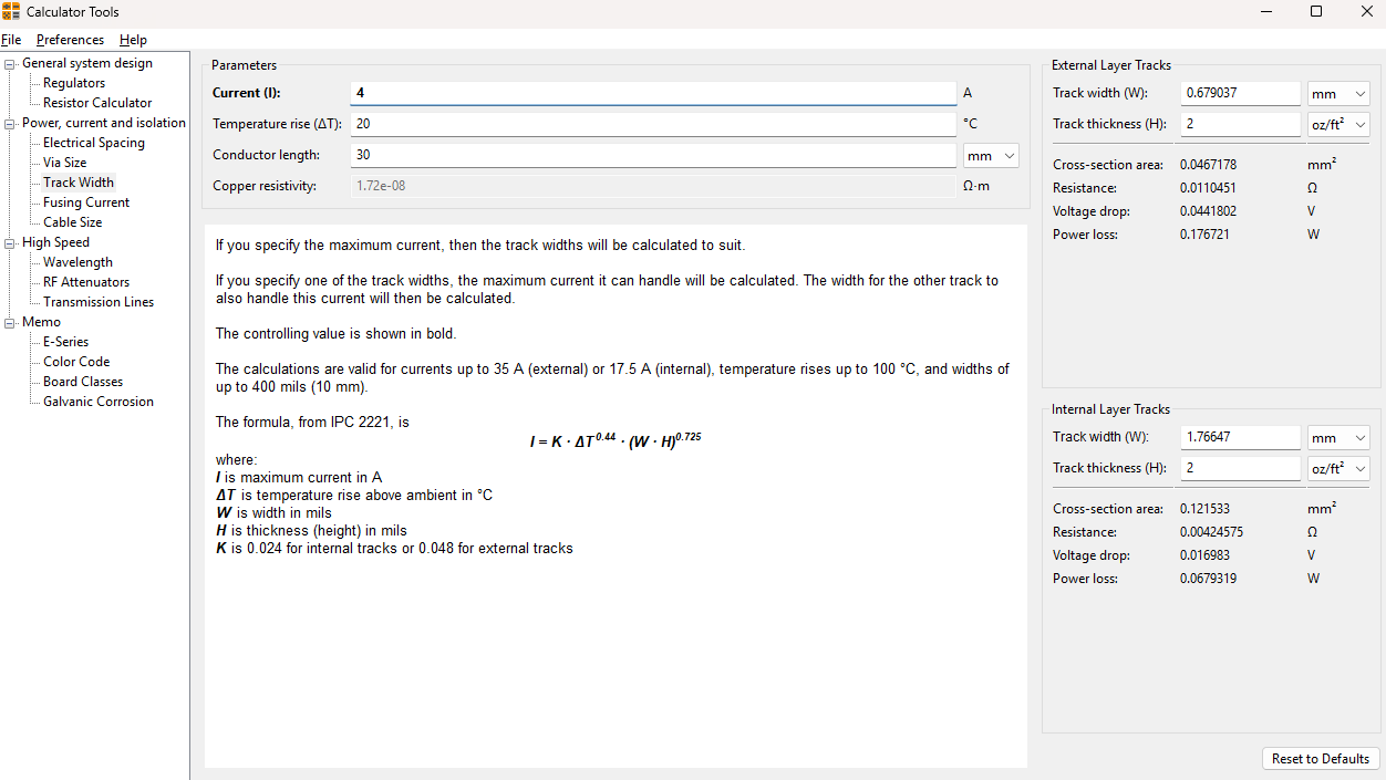
Since the temperature rise and copper weight are set by our 5A traces, we can calculate the trace widths needed for 4A and 2A as 0.7mm and 0.3mm as seen below:

Via Size Calculations
When calculating the Via Size, we can use the 20C temperature rise from the above calculations. We should be careful to not confuse the 2 oz/ft^2 copper weight with the plating thickness of the Via. Using JLCPCB's default capabilities, we can see that the "Average Hole Plating Thickness" is 18um. Keeping all other parameters default in KiCAD, including the default Via Hole Size of 0.4mm, gives us a Via that can support up to 2.4A:
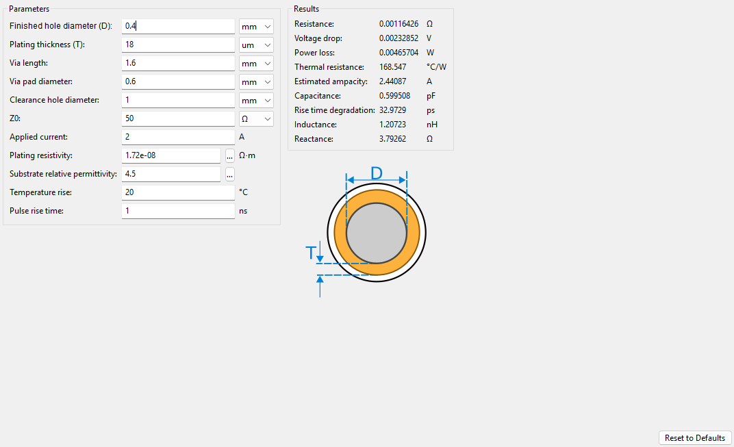
While this will be sufficient for the buck converter 3.3V and 5.0V 2A output domains, the VBUS 5A domain will need larger Vias. Going up by 0.1mm steps, we can arrive at a 1.2mm Via Hole Size which is the minimum Via Hole Size that supports over 5A with a max rating of 5.3A:
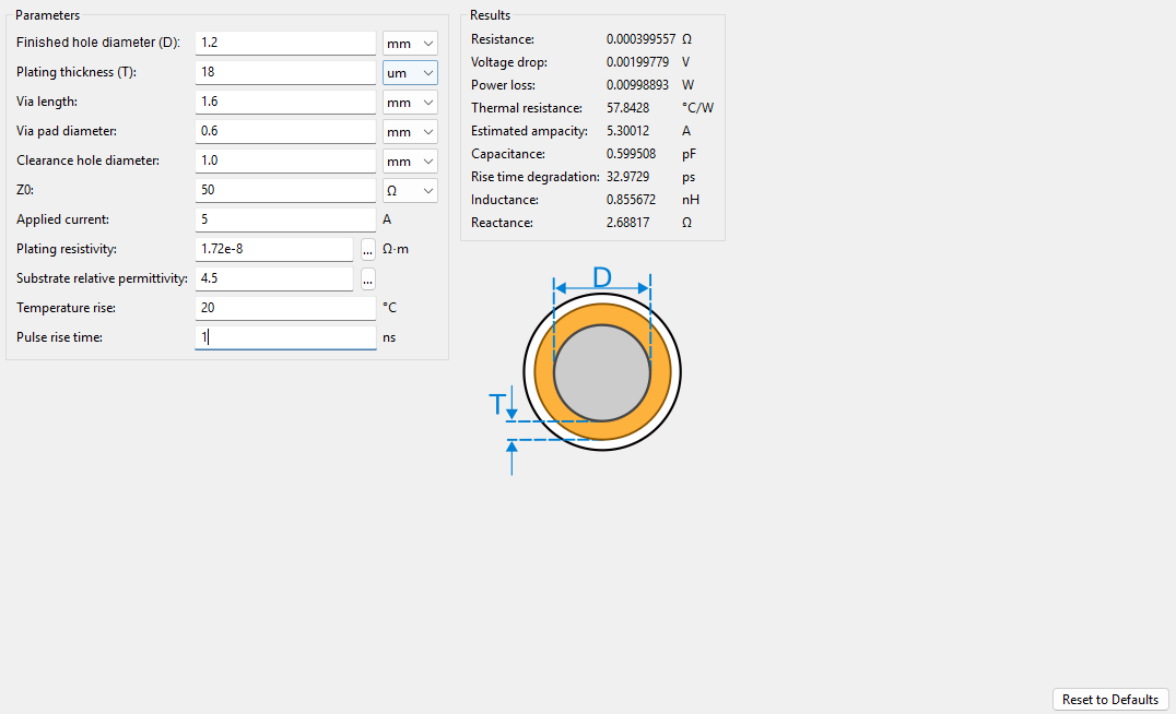
Going forward, we'll use 1.2mm Via Hole Size for both the 4A and 5A Via's to make PCB manufacturing simpler by only having two Via Hole Sizes ( 0.4mm and 1.2mm ).
2 Layers vs 4 Layers
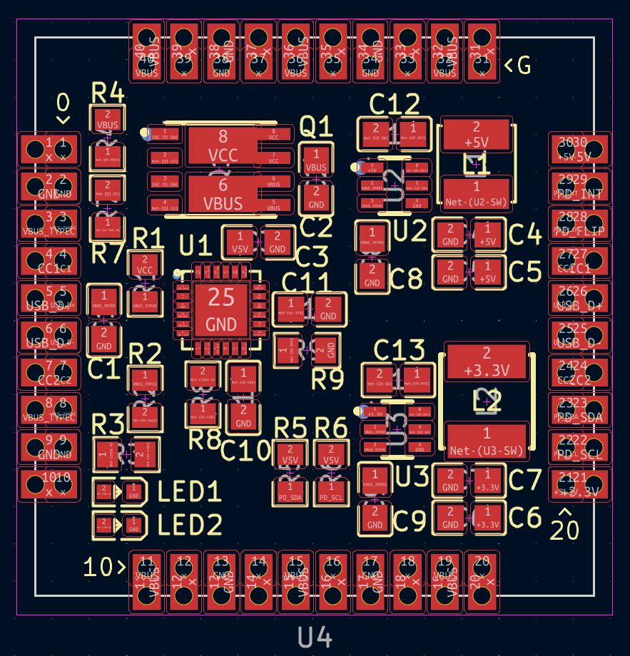
When first starting this project, my goal was to stick to a 2 layer board to reduce cost. However, as I have been attempting the routing, 2 layers has become an unreasonable ask. The main reason for this is due to the size of the board and the widths of the traces. As you can see from above, there isn't much wiggle room left to reduce trace width. We could increase the size of the board, but I want StampPD to be as small as possible. This allows it to be used in as many projects as possible. At 30mm x 30mm, we can fit all of the necessary components on the top of the board so trace routing is the only limiting factor. Trace routing is especially difficult when routing the VBUS output from the back-to-back MOSFET. Since the PCB pin out interface has VBUS output pins on the top and bottom ( image top and bottom, NOT top and bottom layers of the PCB ), the 1.2mm 5A traces intersect with many other traces such as USB D+/- and CC1/2. You can see this below by imagining wires connecting the PCB VBUS pins ( pins 11, 15, 19, 32, 36, 40 ) and the MOSFET ( Q1 ) VBUS pins ( pin 6 ):
To solve this issue, StampPD will be a 4 layer board with dedicated ground and VBUS power layers, stacked from top to bottom as: Top Component Layer -> Ground Layer -> VBUS Layer -> Ground/Signal Layer. The dedicated VBUS layer will connect the output of the back-to-back MOSFET to all VBUS output pins. Since the internal layers of a PCB are usually 0.5 oz/ft^2 and have less ability to dissipate heat, the VBUS layer should be as free of traces as possible. Using the KiCAD Trace Width Calculator with 5A, 20C temperature rise, and 0.5 oz/ft^2 give us a trace width of 9.6mm for internal traces. Since there will be dedicated copper across almost all of the 30mm x 30mm VBUS power layer instead of direct traces, a dedicated VBUS power layer seems reasonable. Note that we will still need to route 5A traces for VBUS input to the VBUS_TypeC Input Domain and MOSFET VCC input on the top/bottom layers so all of the calculations above are relevant.
Summary
Traces
All Traces assume 20C Delta with 2 oz/ft^2 copper thickness for Top/Bottom Layers:
- 2A - 0.3mm Trace Width
- 4A - 0.7mm Trace Width
- 5A - 1.2mm Trace Width
Vias
All Vias assume 20C Delta, 18um Plating Thickness:
- 2A - 0.4mm Hole Size (Diameter)
- 4A and 5A - 1.2mm Hole Size (Diameter)
- Combine 4A and 5A Via sizes to reduce number of Via Holes Sizes needed ( cheaper! )
PCB Layers
- Top Component Layer ( 2 oz/ft^2 )
- Ground Layer ( 0.5 oz/ft^2 )
- VBUS Power Layer ( 0.5 oz/ft^2 )
- Bottom Signal/Ground Layer ( 2 oz/ft^2 )
Discussions
Become a Hackaday.io Member
Create an account to leave a comment. Already have an account? Log In.