 Alec Probst
Hello all,
In this log I'll go over the specific component selection for the 5.0V and 3.3V Buck Converters. Since I am using the same IC for both 5.0V and 3.3V, most of the components will be duplicated between the IC's. Only the inductors will be different between the two implementations.
Buck Converter IC Selection
The main buck converter IC is the AP6300. This IC comes in a couple different flavors including a 3.3V ( AP63203 ) and a 5.0V ( AP63205 ) version which I've selected for StampPD. Some reasons I've selected this IC were:
- Supports input voltage between 3.8V to 32V as StampPD will support between 5.0V and 28V input
- Continuous Output Current of up to 2A which is likely overkill but I want to be able to use StampPD in almost any project
- Allows for 100% Duty Cycle Operation and should allow for close to 5.0V output when there is 5.0V input, similar to an LDO!
- Decently efficient ( >85% ) for a range of output currents in both 3.3V and 5.0V
- Two different fixed voltage versions means I can duplicate some of the work designing the circuits since they are similar
- Fixed voltage versions means I can remove resistors that would be used to define the output voltage and save PCB area
- TSOT23-6 package is reasonable small yet still hand solderable
- Relatively cheap on Digikey ( ~$0.71 ) and JLCPCB ( ~$0.36 )
- Enough quantity on Digikey ( >12,000 ) and JLCPCB ( >30,000 ) to not worry about supply
- Thorough documentation including efficiency curves, an example circuit, PCB layout recommendations, and recommended component values and calculations.
Efficiency and Output Voltage
Below are the efficiency, load, and line regulation curves for the AP6300. Figure 4 shows the efficiency at different output current for 12V, Figure 5 shows the efficiency at different output currents at 24V. The blue line is 5.0V output, the red line is 3.3V output. Figure 6 shows the expected output voltage at different currents. The blue line is input voltage of 12V, the red line is input voltage of 24V. Figure 7 shows the expected output voltage with different input voltages. The blue line is output current of 1A, the red line is output current of 2A. From these we can take away a couple things:
- Ideal current draw is between 0.2A and 2A for >85% efficiency
- This is true for both 12V and 24V input and 3.3V and 5.0V output
- I expect most applications of StampPD to be within this range
- Output voltage for 5.0V will likely be between 5.06V and 5.19V for different output currents
- There will be lower output voltage as output current increases
- Trend between the lines shows that likely closer to 5.19V at lower output currents and voltages
- No data for 3.3V
- Output voltage for 5.0V will likely be between 5.03V and 5.20V for different input voltages
- There will be lower output voltage as input voltage increases
- Trend between the lines shows that likely closer to 5.20V at lower input voltages
- No data for 3.3V
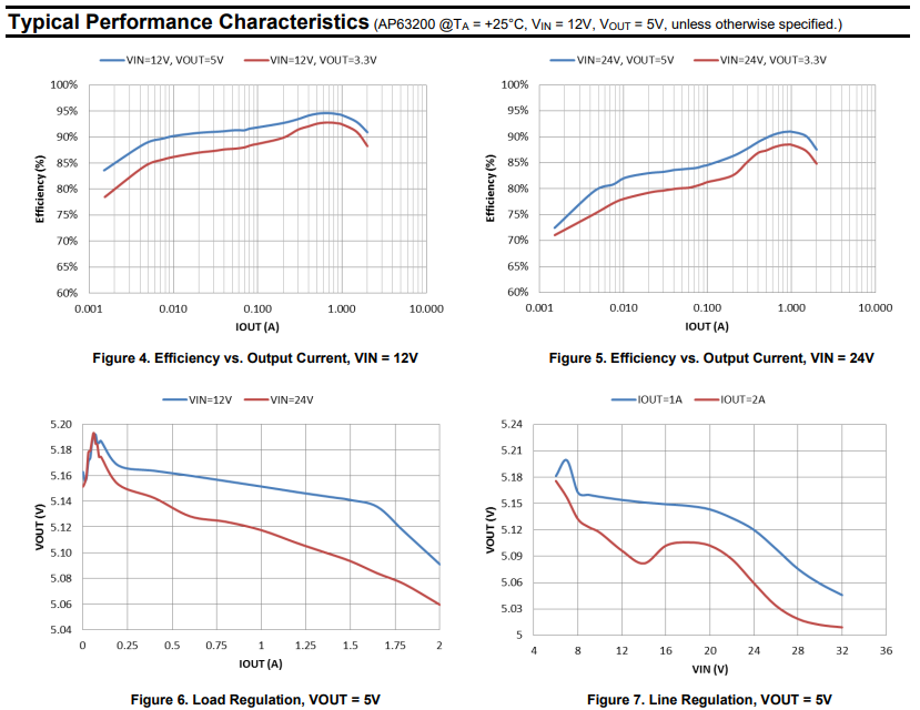
I expect that for the 5.0V AP63205 I should see around 5.20V at low input voltage and low output current. As the input voltage and output current increase, I expect the output voltage to drop to just above 5.0V.
Using the efficiency trends in Figure 4 and Figure 5, I will guess that voltage for the 3.3V AP63203 will likely be worse (higher voltage at lower output currents and input voltages). Using the efficiency percentage difference of around 5% in Figures 4 and 5, and the voltage difference of around 0.2V from Figures 6 and 7, assuming this IC outputs 3.3V at around 2A 32V input, I calculate an output voltage around 3.3V + 0.2V * 1.05% = 3.51V.
I expect that for the 3.3V AP63203 I should see around 3.51V at low input voltage and low output current. As the input voltage and output current increase, I expect the output voltage to drop to just above 3.3V.
Recommended Components
Below, an example circuit, called Figure 1, shows what an implementation of the AP63205 should look like. Two tables, called Table 2 and Table 3, show recommended component values. Table 2 show the components for the AP63203 while Table 3 is for the AP63205.
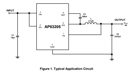
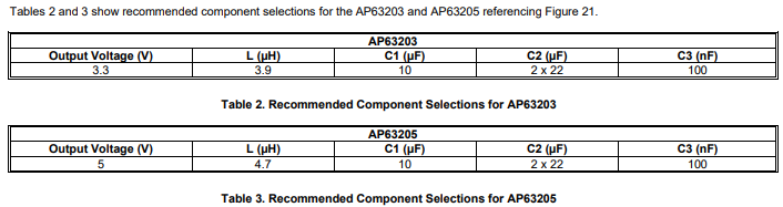
As you can see from the Table 2 and Table 3, the capacitors for both AP63203 and AP63205 have the same recommended capacitance. Only the the inductors have different inductance values. This means we can use the same capacitors between both implementations and only change the inductor.
Capacitor Specifications
For the AP6300 we have 3 different types of capacitors: Input ( C1, 10uF ), Output ( C2, 22uF ), and Bypass ( C3, 0.1uF). The input capacitor stabilizes input voltage and suppresses high frequency noise, the output capacitor stabilizes output voltage and reduces ripple current, and the bypass capacitor stabilizes voltage and suppresses high frequency noise for the AP6300's internal circuitry.
Since all capacitors here are being used for high frequency application, Multi-Layer Ceramic Capacitors ( MLCC ) with X7R or X5R dielectric are a good choice. MLCC's have a low Equivalent Series Resistance ( ESR ) , ie the amount of resistance a capacitor has.
For the input capacitor of 10uF, this capacitor is expected to see at least 28V from the USB-PD circuit. Using a voltage rating rule of thumb of >=1.5x expected voltage, we should choose a voltage rating 28V * 1.5 = 42V. Most capacitors won't have voltage rating of this exact number so I round up to >=50V.
For the two output capacitors of 22uF, these capacitor is expected to see at least 3.3V or 5.0V from the output of the AP6300. Using a voltage rating rule of thumb of >=1.5x expected voltage, we should choose a voltage rating 5.0V * 1.5 = 7.5V. Most capacitors won't have voltage rating of this exact number so I round up to >=10.0V. Note that we're using two 22uF capacitors here as that increases the capacitance and reduces the ESR at the cost of an additional component and board space. Capacitance in parallel is additional ( Ex: Ctotal = Ca + Cb ) while resistance decreases by the reciprocal of the sum ( 1/Rtotal = 1/Ra + 1/Rb ).
For the bypass capacitor of 0.1uF, this capacitor is between two pins on the AP6300, SW and BST. SW has a voltage (Vsw) between -1.0V and Vin + 0.3V. BST has an voltage (Vbst) of Vsw - 0.3V to Vsw + 6.0V. Since this capacitor is between these two pins and not ground, we only care about the maximum difference in the voltage between SW and BST. Since Vbst is always related to Vsw, we know that the maximum voltage difference is 6.0V, even if the voltage difference to ground may have a maximum value of Vin ( 28V ) + 0.3V + 6.0V = 34.3V. Using a voltage rating rule of thumb of >=1.5x expected voltage, we should choose a voltage rating 6V * 1.5 = 9V. Most capacitors won't have voltage rating of this exact number so I round up to >=10V. The bypass capacitor is particularly important here as drops in voltage or current can cause glitches and instability in the AP6300.
Inductor Specifications
There are two different Inductors needed for the different IC's, 3.9uH for the AP63203 and 4.7uH for the AP63205. The inductor for the AP6300 in this circuit stores and releases energy to help smooth the voltage and current load. These inductors will likely be the largest components on the board.
Since we're implementing two of these on a single PCB close together and it's unknown what other circuits StampPD will be used with, we will want shielded inductors. This contains the magnetic field of the inductor and reduces electromagnetic interference between the other inductor as well as any other devices around them.
Inductors have two different current ratings: A saturation current ( Isat ) and a RMS current rating ( Irms ).
The Isat is the maximum current the inductor can handle before its magnetic material is saturated and it can't store energy efficiently. If we send this amount of current through the inductor, we will have reduced efficiency compared to the curves we looked at above due to reaching the limits of the magnetism of the inductor. Based on the maximum peak current ( Ipeak_limit ) in the Electrical Characteristics of the AP6300, we will see a Ipeak_limit of 3.1A. Using a rule of thumb of 30% safety margin for inductor current, we should choose a saturation current of 3.1A * 1.3 = 4.03A. For simplicity, I round down to 4A
The Irms is the maximum current the inductor can handle before it passes a thermal degradation limit. If this amount of current is reached, the inductor will start to degrade due to heat melting parts of it. To calculate the Irms, we can use the equation:
Irms and output current will be in amps while inductor ripple current will be in volts.
We know the Output Current is 2A but we need to calculate the Peak-to-Peak Ripple Current ( Irpl ) using the equation:
Irpl, output voltage, and input voltage will be in volts, inductance in henry, and switching frequency in hertz.
With this, we can see we need to calculate two different Irpl for the AP63203 and AP63205 as we have different output voltages and inductance values.
For the AP62303 we have a 3.3V output voltage, 28V maximum input voltage, 3.9uH inductance, and 1.1MHz switching frequency. This gives us a Irpl = 0.67857142857A:
Using the Irms equation with 2A output load current and Irpl of 0.67857142857A, we get an Irms of 2.00957000342A:
For the AP62305 we have a 5.0V output voltage, 28V maximum input voltage, 4.7uH inductance, and 1.1MHz switching frequency. This gives us a Irpl = 0.79441834761A:
Using the Irms equation with 2A output load current and Irpl of 0.79441834761A, we get an Irms of 2.01310499211A:
With the Irms calculated, we can now apply the 30% safety margin for inductor current and round down for a AP63203 Irms of 2.00957000342A * 1.3 = 2.6A and AP63205 Irms of 2.01310499211A * 1.3 = 2.6A. These values happen to round out to the same which means we only need to look for a difference in inductance between our inductors!
Component Summary
5.0V Buck Converter
- 1x AP62305
- WU-7 version is ok, QWU-7 is automotive grade
- 1x 10uF Capacitor
- Ceramic MLCC
- X7R or X5R Dielectric
- At least >=28V, recommended >=50V
- 2x 22uF Capacitors
- Ceramic MLCC
- X7R or X5R Dielectric
- At least >=5V, recommended >=10V
- 1x 100nF Capacitor
- Ceramic MLCC
- X7R or X5R Dielectric
- At least >=9V, recommended >=10V
- 1x 4.7 uH Inductor
- Shielded Inductor
- At least >=3.1A saturation current, recommended >=4A
- At least >=2A RMS current rating, recommended >=2.6A
3.3V Buck Converter
- 1x AP62303
- WU-7 version is ok, QWU-7 is automotive grade
- 1x 10uF Capacitor
- Ceramic MLCC
- X7R or X5R Dielectric
- At least >=28V, recommended >=50V
- 2x 22uF Capacitors
- Ceramic MLCC
- X7R or X5R Dielectric
- At least >=5V, recommended >=10V
- 1x 100nF Capacitor
- Ceramic MLCC
- X7R or X5R Dielectric
- At least >=9V, recommended >=10V
- 1x 3.9 uH Inductor
- Shielded Inductor
- At least >=3.1A saturation current, recommended >=4A
- At least >=2A RMS current rating, recommended >=2.6A
Discussions
Become a Hackaday.io Member
Create an account to leave a comment. Already have an account? Log In.