 Alec Probst
Hello all!
It's been a second since the last log. I have been busy with end of the year plans and have finally come back to this project. Progress has not stopped while I was away though!
In this log I'll go through my methodology when ordering EVT (Engineering Validation Test) Components and PCBs, reasoning for chosen Component Suppliers and PCB Fab, and some changes to the PCB as a result.
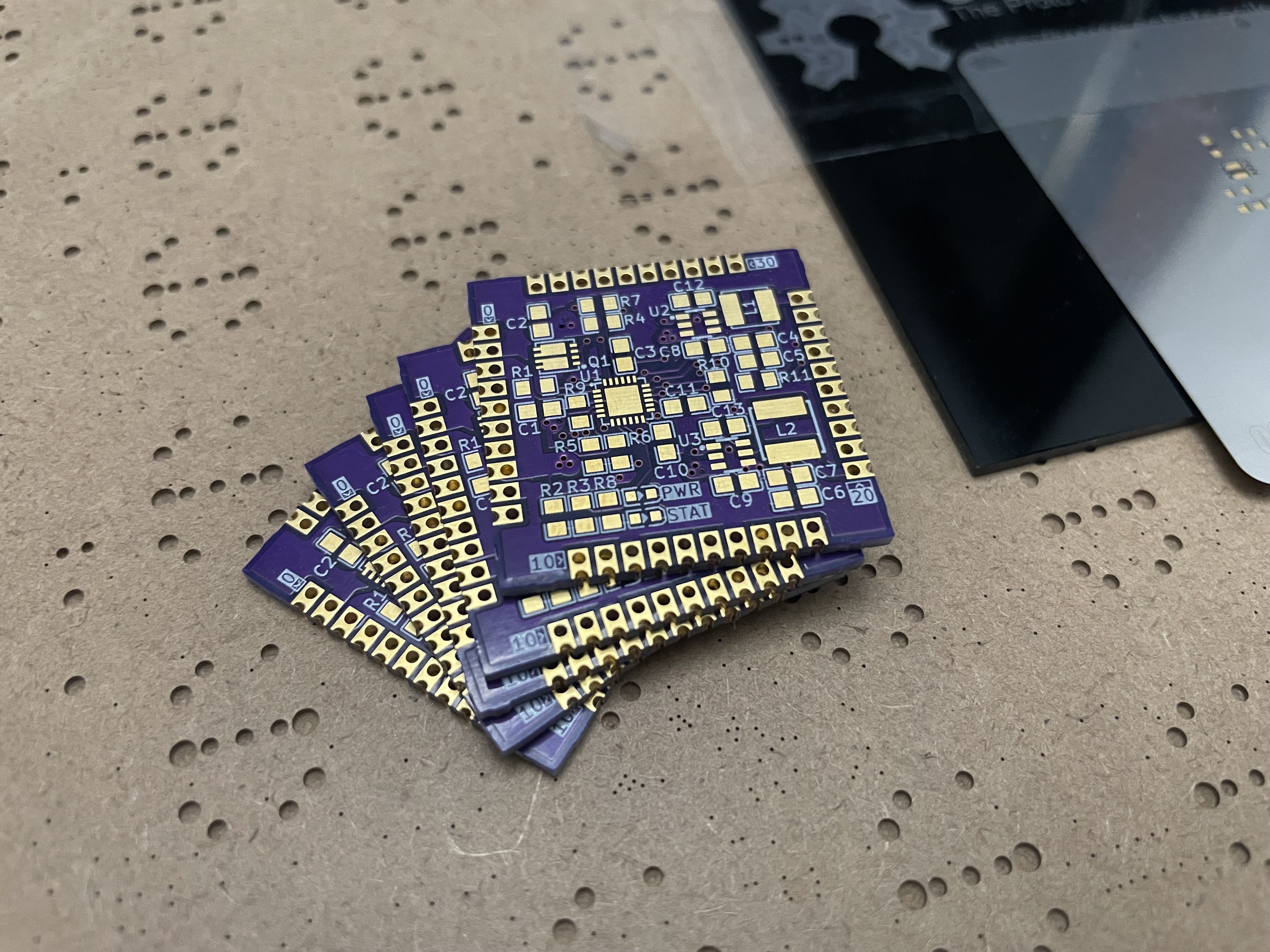
Sneak Preview of the PCBs!
EVT Decision Methodology
My goal for EVT is to test the PCB and Components to make sure StampPD works correctly. I also want to validate some cost cutting decisions for the PCB that will be explained below. For the EVT iteration I will be hand assembling PCBs to get an understanding of component assembly issues, silkscreen confusion, and to make any necessary PCB fixes easier. My target quantity of StampPD EVT boards is 10 working prototypes but I ordered Components/PCBs for 12 boards to account for mistakes, broken components, and potential destructive testing.
EVT Component Supplier Choice
The conclusions from the "DIY Component Cost Comparison" log have remained the same. I ordered all passive components from LCSC and 4 IC components from Digikey. The total cost of components can be seen below:
- Passive Components - $22
- $10 for components
- $12 for shipping, tariffs, and tax
- IC Components - $48
- $36 for components
- $12 for shipping, tariffs, and tax
- Total Cost for all Components - $70
- $46 for the raw component cost
- $24 for the shipping, tariffs, and tax
EVT PCB Fab Choice
One decision that has changed from past logs is the PCB Fab. Originally I was planning to use JLCPCB or PCBWay as they were the cheapest based on my calculation of x100 PCBs. However, JLCPCB and PCBWay had additional tariffs well over $200 at the time I was ordering PCBs. Instead I used OSHPark as my PCB Fab and OSHStencil as my Stencil Fab since they are an American company and do not have tariffs. OSHPark was originally not considered in the "PCB Fab Cost Comparison" log due to their limited PCB options. The cost increase from the tariffs helped spur on some of the PCB changes below to manufacture the PCB with OSHPark. The total cost of the PCBs can be seen below:
- PCBs - $56
- Free Shipping
- Stencil - $15
- $10 for stencil
- $5 for shipping
- Total Cost for PCBs and Stencil - $71
Total Cost for EVT Prototypes - $141
- Raw Component/PCB Cost - $112
- Shipping, Tariffs, Tax - $29
Copper Weight
In the "PCB Trace/Via Calculations and 2 vs 4 Layer PCB" log I chose 2 oz/ft^2 for the top and bottom layers of the PCB as it allowed for smaller trace widths. OSHPark 4 layer boards only have the option for 1 oz/ft^2 top and bottom copper thickness and 0.5 oz/ft^2 middle layer copper thickness. This increases the Trace Widths of the design!
Trace Width
With the decrease in copper thickness, the Trace Widths on the Top and Bottom layers needed to increase. To facilitate this, I moved the 5A net to Top layer and 4A net to Bottom layer. The 2A traces remained on the Bottom layer like before. This minimized the size impact of these traces and allowed for the PWR layer to be an unbroken plane. Shuffling some components and traces around allowed the PCB to remain the same 30mmx30mm size constraint.
- 2A - 0.3mm -> 0.7mm Trace Width
- 4A - 0.7mm -> 1.5mm Trace Width
- 5A - 1.2mm -> 2mm Trace Width
Via Hole Size
When looking at the manufacturability of the PCB, I realized just how big the 1.2mm Via Hole Size was for the 5A and 4A nets. These holes takes up a lot of space and could cause shorting issues. To resolve this, I replaced the 1.2mm Hole Size with x3 0.4mm hole size. This reduced the number of drill sizes need to 2 and allows for all Vias to be tented at the cost of more drilled holes per PCB. They should be able to carry the same amount of current.
- 4A and 5A Via Hole Size - 1.2mm -> x3 0.4mm
EVT Testing Concerns
As I assemble and test the EVT PCBs, I will be keeping an eye on the PCB thermals. I have concerns about how close some of the components are, traces getting too hot, and the internal PWR layer getting warmer than expected in certain areas due to Vias "pinching" specific sections of copper on the PWR plane.
Discussions
Become a Hackaday.io Member
Create an account to leave a comment. Already have an account? Log In.