 deftcoyote
Currently, the standard protoboard landscape looks like this:
- protoboard - I believe is a general term for any type of development board
- perfboard - a board of individual plated holes. Allows for arbitrary layout, but requires adding wiring between all components, which can get obnoxious.
- stripboard/veroboard - a board with rows of copper connected holes. Even though they are useful for connecting components, if you don't need all the holes, you either have to waste them or cut the traces, which are usually thick.
- bus - a combination of connected and disconnected holes similar to breadboard patterns. The best hybrid option, but still requires wasting many holes due to the track they're on, or because of the layout.
- other - there are many different combinations/patterns of strips and individual holes for different types of circuits.
Some notable recent developments on prototype boards:
- Perf+ (https://www.crowdsupply.com/ben-wang/perf-2). This is a perfboard with a adjacent solderpads that connects it to either a horizontal or vertical strip/bus. This allowed easy connection between any 2 points with just a couple of solderpad connections. However, both strips are now in use and any other connection must take this into account. Also, it makes following the circuit difficult.
- Bread2Board (https://www.kickstarter.com/projects/jamescaska/bread2board-desktop-diy-circuit-board-printer). Taking the basic matrix idea of an FPGA to a breadboard. Solderpads make the connections and you can lay things out fairly easily. However, debugging is difficult, and it requires very complicated boards.
- RoutaBoard (https://hackaday.io/project/11911-routaboard). This is a essentially what I want to make (for the additive version) with standard DIP pin distance. However, the routing is not always obvious, it seems to be out of production, and the files are not available. Also, given how close all the pads are, it seems possibly prone to shorts.
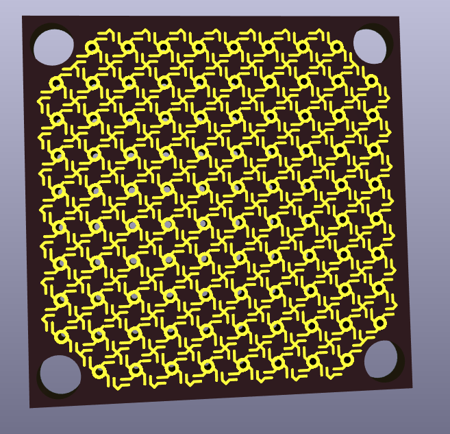
I think all of these are great, but the first two are complicated because the wiring is not straightforward. It left me thinking that it would be easier to just assume a single (or double) layer board with direct connections to neighbors. If the hole isn't used, it still passes on the signal. Thus, a line of holes connecting components is the same as a wire. It's just standard planar circuit layout on a grid.
There are 2 useful ways to do this:
- Everything is disconnected like a perfboard. Each hole has solderpads to its 4 (or 8 with diagonals) neighbors. Once components are in place, just solder the pads along a route between the two pads to be connected. The downside is it spreads everything out due to the solderpads.
- Everything is connected with thin traces. Any connection you don't want is easily severed with an exacto knife or dremel. This allows the board to stay small, but requires cutting a lot of traces before adding components.
These fix the need for any wiring while allowing easy to follow traces with arbitrary layouts. For the connected one, the traces are easy to cut.
I knew projects like the RoutaBoard existed, but could not find any. Conceptually, the RoutaBoard is everything I want, but has large tracks and large pads leaving incredibly small tolerances, which might be easy to make a short. I'm using small traces to hopefully prevent this and direct routing. Also, with no way to purchase or have the RoutaBoards made (no files), it's still not a viable option.


 deʃhipu
 Alan Green
 Ben Holmes
 Ted Yapo
Recently I learned about acrylic scoring knives. One of those might make quick work of isolating a connected path from an all-connected board. And make the certainty of isolation cuts easier to inspect vs cuts with a simple sharp knife.
https://duckduckgo.com/?q=acrylic+scoring+knife
If it works, that might reduce the usability penalty for connecting diagonals too.