 Anders Helgesson
I rearranged the design so it's much more easy to see what is going on inside the SLG46582 PowerPAK.

Turned the I2C registers into network labels instead to remove a lot of lines, makes it a bit easier to see what is going on. The SEL0 and SEL1 logic was moved into its own area since it's logic is separated from the other logic.
The internal design is nothing like I expected, the NC pin has functionality to it. One of the I2C level shifter control pins are not set up as an NMOS. This can only mean one thing, is this preprogrammed design is an old one? Which is probably the design of GSD Rev 1.0. Quick search online for the user manual for GSD Rev 1.0 and it confirmed that this is probably true. It confirmed the error in the GSD Rev 2.0 manual I found before.
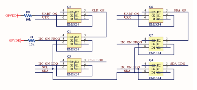
The SEL0, SEL1 and NC Logic
Now before analyzing I have to understand how the logic works inside the GSD PowerPAK. It's hard to reason what happens during analysis otherwise.
Since I want to know what SEL0 and SEL1 does, I'll start looking at the logic that is connected to these pins.
NC, SEL0 and SEL1 is connected to three 3-bit LUTs, 3-L3, 3-L1 and 3-L4.

NC pin is high when only SEL1 is high.
I2C_ON_PROG is only high when SEL0 is HIGH and SEL1 is LOW.
I2C_ON_LDO is HIGH if both SEL0 and SEL1 are low.
So since no more logic is connected is quite easy to reason about the default implementation we have here.
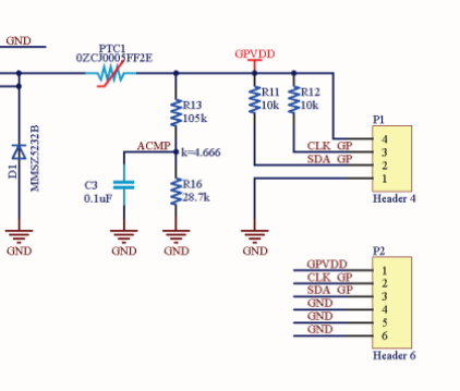
I2C_ON_PROG pin is set up as a open-drain NMOS. This means that if this pin is HIGH it will sink the VDD/EN of the target PCA9306, turning it off.
I2C_ON_LDO pin is set up as a normal output pin. Now we need to look at the schematics again.

The LDO level-shifter can not be turned off in this configuration? It shouldn't matter if I2C_ON_LDO is HIGH or LOW? It's powered through VDD anyway.
Looking at the GSD Rev 1.0 level-shifters
It fits the logic much better. Notice the level-shifter UART pins. NC is UART_ON.
Look at the output here.
There is a 6 pin header there. But with 2 extra GND. Probably where UTX and URX would have gone if they had added UART.
Here is a board view of the GSD Rev 1.0

The final design doesn't include the 2 UART level shifters. So the UART lines are probably not routed at all. The schematic is not updated to fit the final design which is weird. I guess the schematics, board design and documentation was managed by different people. It's only way to explain this.
Looking at this it confirms that the OTP memory logic of the SLG46582 on my GSD Rev 2.0 is the GSD Rev 1.0 design. They probably had a lot of preprogrammed chips to use. Now does this mean that the device is reconfigured by software before it's used?
The Error pin
This probably has the most logic connected to it. Let's start from the error pin and go backwards to the source of the logic.
The output of the Error LUT (3-L0) goes to the Error pin (Pin 4), Status LED LUT (2-L2) and the FET LUT (2-L1).
Let's look at the FET LUT (2-L1) First.
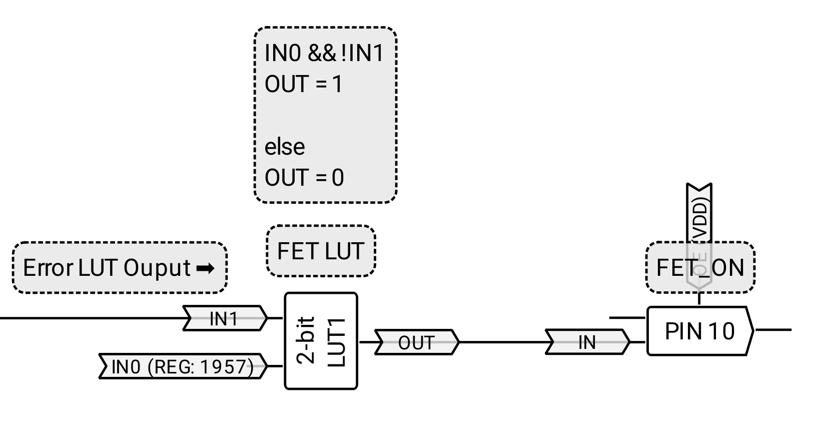
If there is an error, FET LUT output is turned off, FET LUT is controlled directly by the I2C Register 1957.
Next the Status LED.

Here an error turns off the Status LED.
Next is the Error LUT.
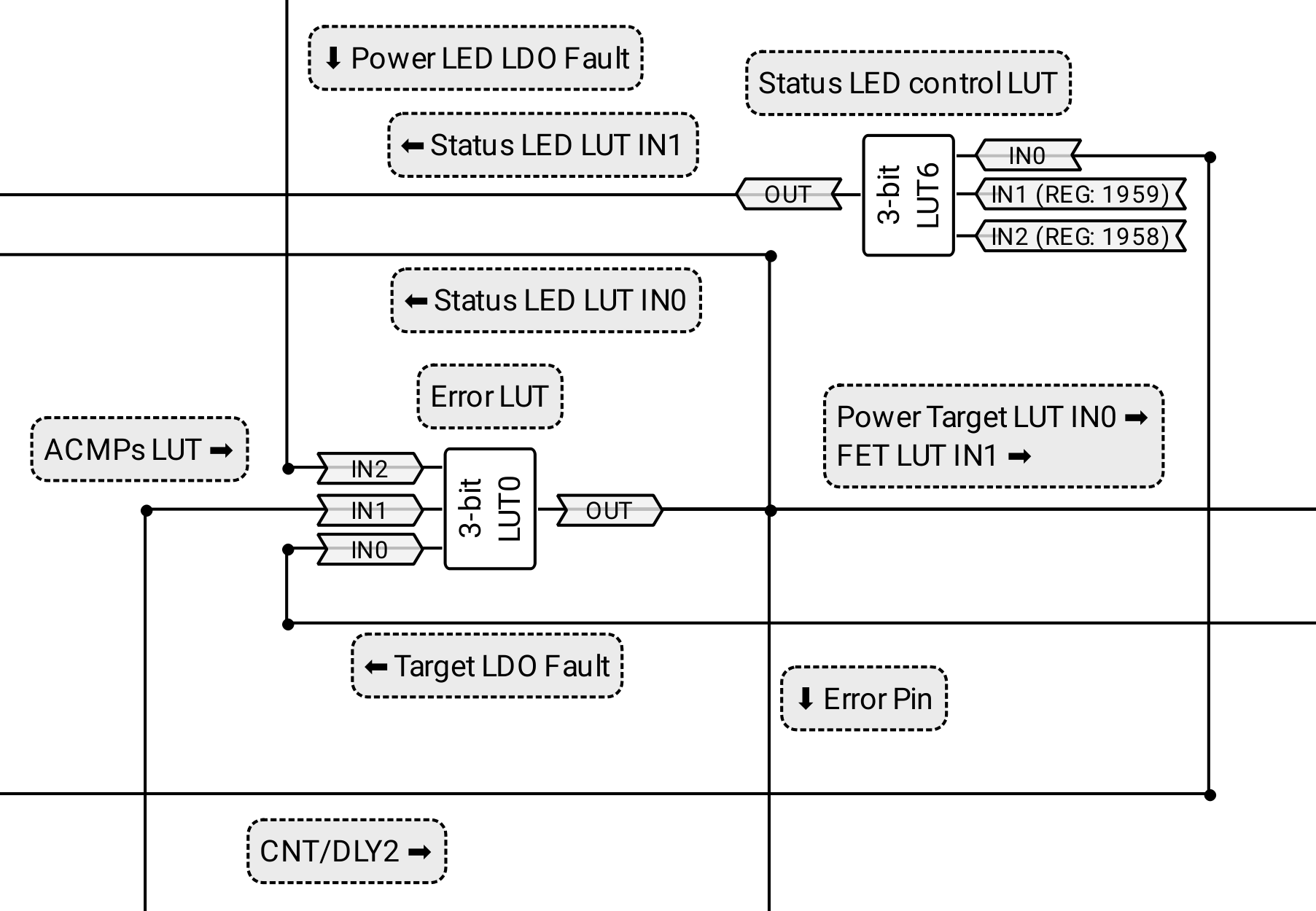
The Error LUT (3-L0). When an error is detected by the logic both the Power target LDO and Target power FET are turned off. The error signals comes from the LDO's themselves (IN0 and IN2) and the ACMPs (IN1). Both overvoltage (ACMP0) and the set temperature limit which is 75 °C (ACMP2).
The status LED control LUT (3-L6). The CNT/DLY2 signal controls the status LED blinking speed. There are two I2C registers connected to it 1958 and 1959.
The I2C register 1958: This controls if the status LED indicator should be on or not.
The I2C register 1959: It controls two things when it's turned on. It releases the powerdown of the OSC1 and enables blinking of the Status LED.
The rest
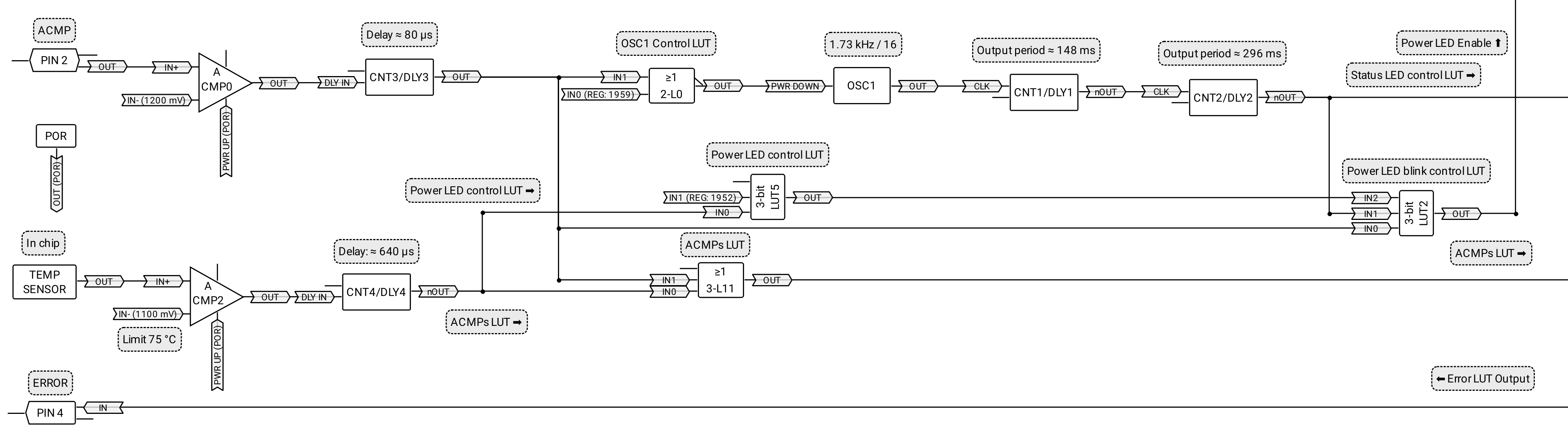
ACMP0 is use for overvoltage if overvoltage is detected it will make the power LED blink and activate the ACMPs LUT which signals an error.
ACMP2's output is activated if the temperature sensor in the chip reaches more than 75 °C, it will turn off the Power LED and activate the ACMPs LUT which signals an error.
OSC1 Control LUT turns off the OSC1 if both inputs are 0.
OSC1 has the clock divided down using 2 delays so that you can see the LEDs blink when used.
Here is the complete design in datasheet style with my comments.

I probably missed something but we should now know how the PowerPAK logic works in the GSD Rev 1.0. Now we have to know how the device is reconfigured for the GSD rev 2.0 hardware. There are two ways this can be done I guess.
- Capture dumps. Analyze them all to try to find when it's reconfigured.
- Use the GSD Rev 2.0 and dump the PowerPAK afterwards.
Since we don't know when it's reconfigured I'll capture the powerpak logic after it's been used. Fastest and easiest route. If they don't reset the PowerPAK between uses the dump should contain the new design.
Discussions
Become a Hackaday.io Member
Create an account to leave a comment. Already have an account? Log In.