0%
0%
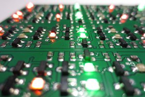
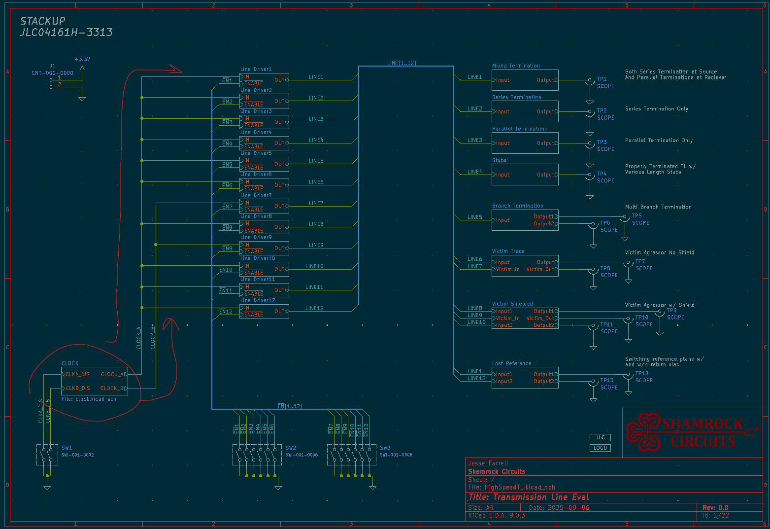
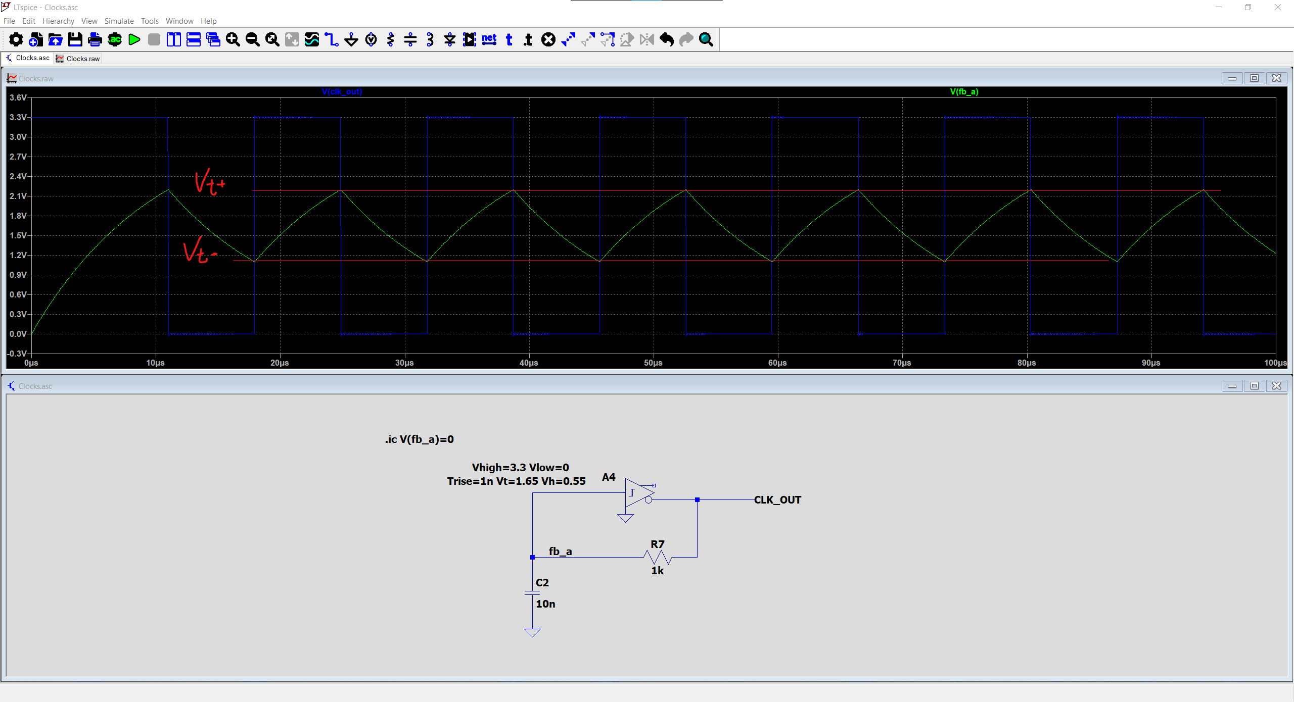
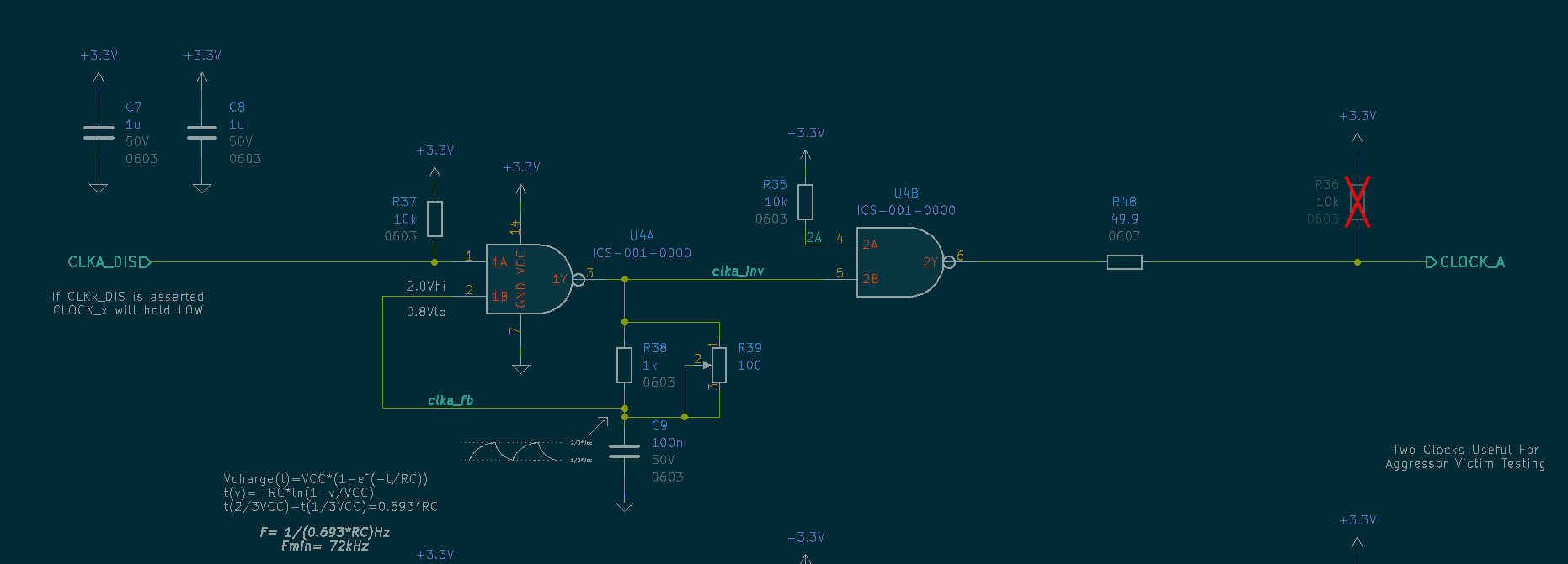
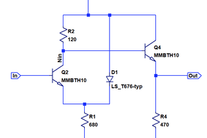
Transmission Line Test Board
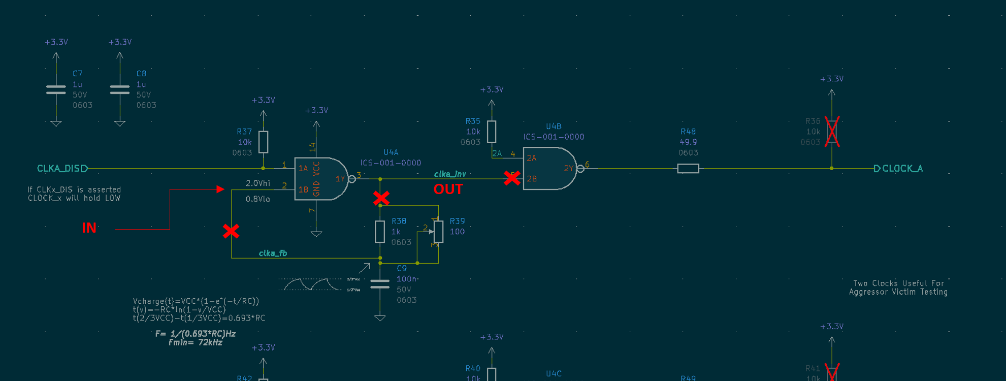
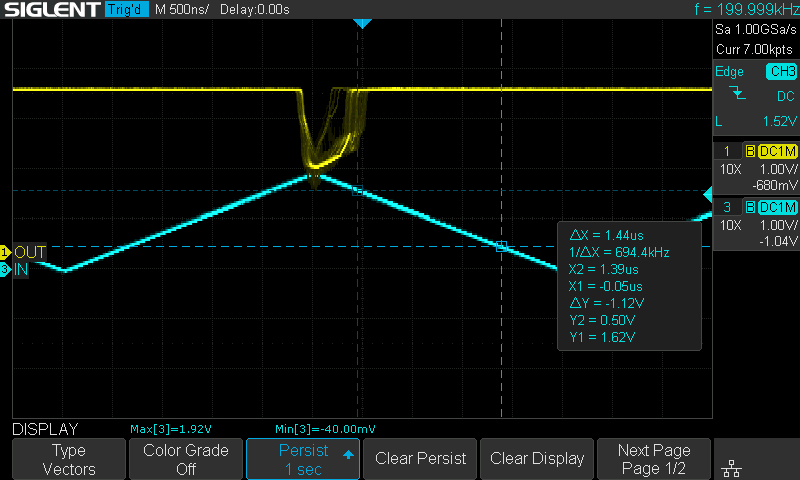
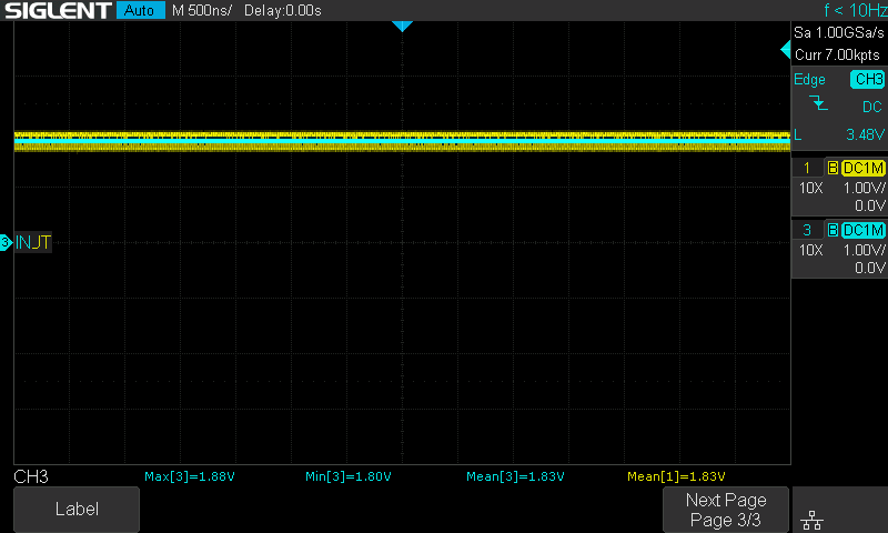
Series, parallel and branch termination. Influence of stubs and reference changes. Aggressor-victim shielding techniques.
 Jesse Farrell
Become a Hackaday.io member
Already have an account? Log in.
Just one more thing
To make the experience fit your profile, pick a username and tell us what interests you.
Pick an awesome username
hackaday.io/
Your profile's URL: hackaday.io/username. Max 25 alphanumeric characters.
Pick a few interests
Projects that share your interests
People that share your interests

 Tim
Tim
 Discrete Electronics Guy
 Yann Guidon / YGDES