The Optical Inch
An approach to entry-level wideband spectrometry (color temperature & CRI, UV-A /UV-B dosimetry, material identification, ...)
An approach to entry-level wideband spectrometry (color temperature & CRI, UV-A /UV-B dosimetry, material identification, ...)
To make the experience fit your profile, pick a username and tell us what interests you.
We found and based on your interests.
20170102 DDC118 basic test.inobasic demo for the Stellaris Launchpad (LM4F120H5QR) that streams rows of tab separated integer values. Use With Energia. Latest version on github!ino - 9.99 kB - 01/02/2017 at 16:58 |
|
The future isn't all that bad when it comes to multispectral multipixel sensors. As for this project: it has been a great journey and inspiration. The new frontier these days is, at least for me, in the short-wave infrared (900-2500 nm), where it becomes ever harder to piece something together with a few photodiodes or LEDs.
Here's to more compact, affordable single-pixel spectrometers, intriguing analog front-end, CCD learning experiences and ubiquitous multispectral imaging, far beyond what The Optical Inch initially set out to do.
Let's enjoy the adorable MEMS Fabry-Pérot interferometer for SWIR spectroscopy, low-cost 10+ channel spectral profiling sensors and lastly the absolutely cool computational approach below that reconstructs spectra based on the responses of definitely-not-narrowband dielectric filters.
Tune in next time when there is a next time! Stay curious.
Kim, C., Ni, P., Lee, K.R. et al. Mass production-enabled computational spectrometers based on multilayer thin films. Sci Rep 12, 4053 (2022). https://doi.org/10.1038/s41598-022-08037-y
A news flash on Hackaday (1) highlights recent work (2) on using Perovskite pixel mosaics to implement multispectral imaging. Similar to Sigma Foveon sensors, layers can be stacked in the optical path to obtain a spectral decomposition of the incident light rays.
The reconstruction is achieved through fitting of a set of coefficients which approximatively encode the inverse transform to the spectral cross-talk owed to overlapping absorbance spectra and incomplete extinction (= "neuromorphic" in fancy-speak).
Depending on the chemical composition, different absorption edges are found:
"Figure S28 displays the testing setup, where we used a projector (M6 Pico Projector, AAXA Technologies) to generate a panchromatic source image and used a lens to focus the incident light onto the chips. Blue, green, and red chips are sequentially stacked (six-terminal stacking) from front to back, where blue, green, and red channels of current are read out independently."
Which is fine for the paper, but points at the compounding difficulty of 2.5D integration - a factor which translates into years of research and a super-linearly growing difficulty in adding more and more spectral bands.
Perovskites are envisioned to be put on plastic foils (3) for solar photovoltaics applications, but here sensors can be kept under vacuum or inert gas in hermetically sealed ceramic packages with glass windows, eliminating some of the stability issues with this class of materials (4):
But if I were to bet, I think it's more likely we'll see Bayer pattern and, at best, 4-6 wavelength sensors with more elaborate CFA-like patterns (5) before high integration happens:
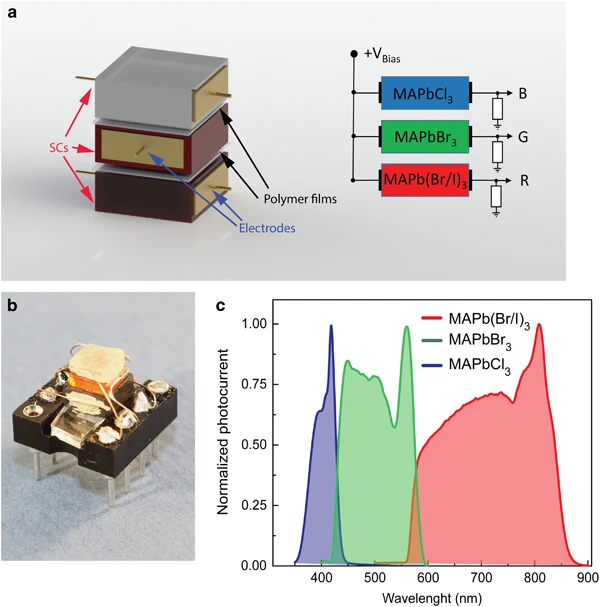
(Note: the C1-C2, C3-C4 and C5-C6 stacked perovskite layers should be similar to gradient engineered light absorption layers, not anti-series diodes. The illustration is a bit strange in that regard. Figures S14 and S15 show adequately contacted organic diode structures as well.)
"Direct contact of perovskite layers appears challenging in the view of known halide-ion mixing. This problem might be mitigated by insertion electrically conductive, optical transparent and halide-ion-impermeable contact layers."
Essentially, some form of mesa etching, passivation, barrier contact formation and metalization would need to take place, as sketched below:
References
of 2 u.fl connectors added instead of 2.54mm pin headers.
3 pin diode array with Pb aperture. Signal GND inside is left disconnected from the sensor head chassis GND and only connected on the DDC118 board.
4 An incomplete iteration - the LDO is still on Rev.1E. Attempts were made :)Should I have a need to build another board, it'll probably look very different today.
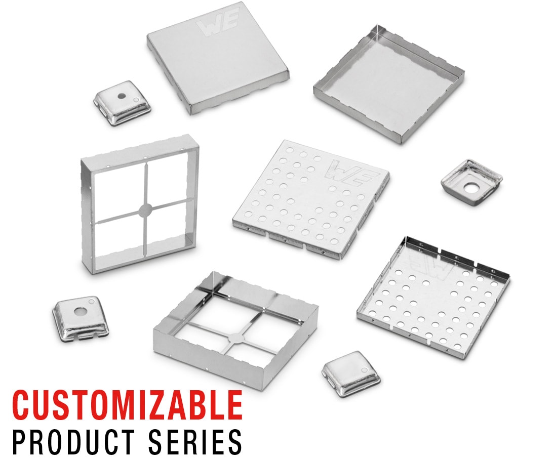
WE-SHC shielding components:
Hirose DF40GL shielded mezzanine connectors:
A recent HaD article highlighted an LED array reflectance sensor for plastics identification. As it's obviously related to this project, I've rummaged around for another source of LED arrays for hyperspectral imaging, absorption / reflection spectrometry and spectral fingerprinting. Check out USHIO's 8-in-1 LED package with a miniature BGA footprint.
It's really becoming clear how these emitters could pave the way for hyperspectral imaging integrated into smartphones, as they are a lot better integrated than single LEDs. Smartphones might even be reworked to replace the LED light / flash with a multi-spectral source for such occasions.
I can also see how a repeating pattern of sequential light pulses can be combined with short exposure times and a rolling shutter sensor to extract a lower-resolution 2D hyperspectral image. Shout-out to [Jerry de Vos], [Armin Straller], and [Jure Vidmar] :)
Here's an inverse solution - when detecting in a wavelength range where LEDs are the go-to light sources and consequently narrow-band, multispectral sensing is easier to do, and the spectral resolution is more sharply defined.
This goes both ways though, as a set of LED dies needs to be available for both photodiode-mode and emitting diodes.
Sometimes I find I entertaining how ideas go full circle. As I was researching some other optical principle, these "multichannel optodetectors" crossed my way. They're effectively what I was striving for with the Optical inch project, albeit at a more reasonable price point than these hermetically sealed optical hybrid modules ;)
Meanwhile I'll keep claiming the approach with LEDs while it lasts.
40x40 mm² stainess square tubing with 8mm tapped holes - one for mounting an aluminium cube, the other to pass the "light" through and the PIN diode array PCB glued to the cube. Add a 1.5x3 mm² pinhole made from 2mm thick lead sheet, light seal all openings with copper tape, Al tape over the pinhole. Done. Note: this is not a transmission measurement but a backscattering geometry.
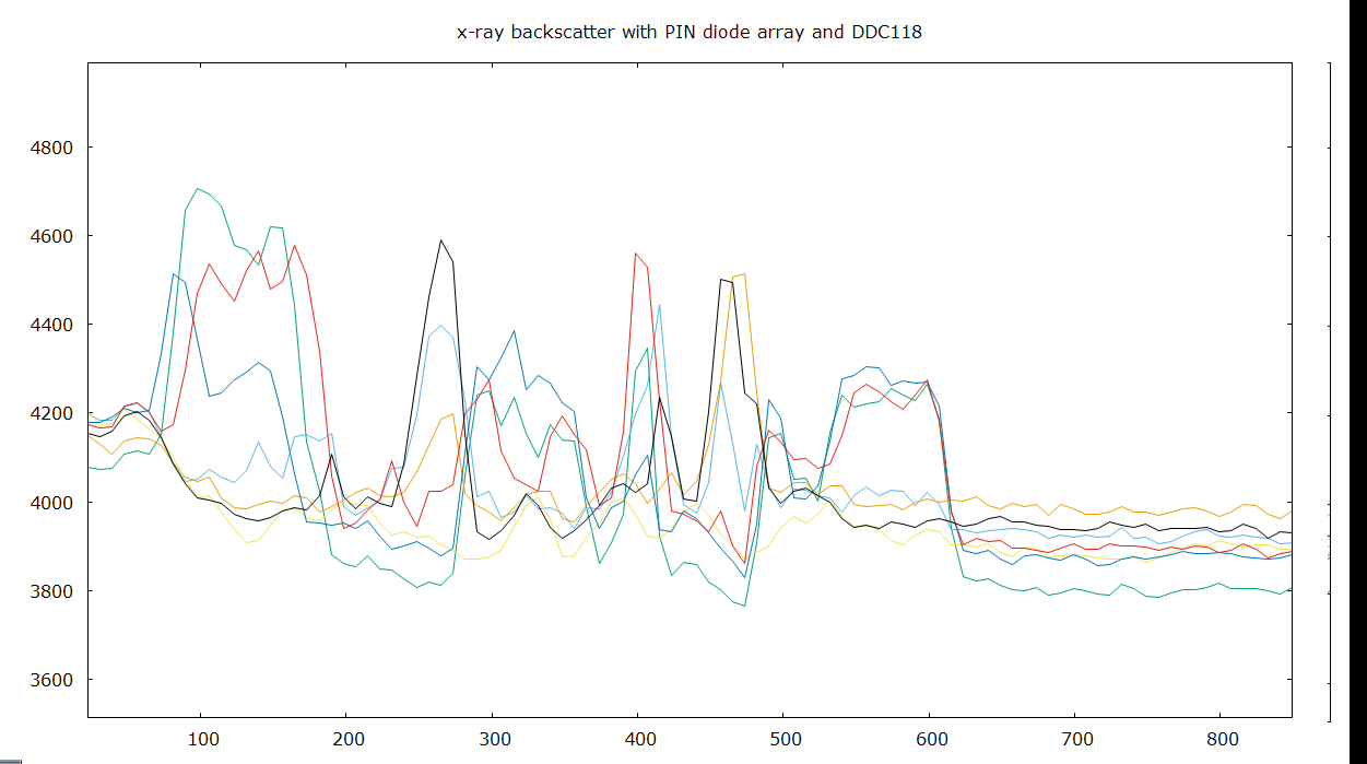
horziontal: time (50ms intervals), vertical: 7 of 8 channels (something went wrong, maybe a connector came off...)

What you see here is the raw 1D image of an 8 pixel x-ray pinhole camera observing a piece of stainless steel illuminated by an x-ray tube ~8cm away as I'm waving it around (duct-taped to a PP tube and held where the dose rate is <2µSv/h).
...And here's just the channels with a bit of smooth kdensity. At approx. sample #610 the x-ray supply is switched off.
It has proven effective to let the analog ground float inside the metal enclosure and connect case GND to the digital ground of the launchpad.
Let me conclude this log entry with a snapshot of the pinhole camera setup. Note this is a different board but I still put that Faraday shield over the exposed input pads. Black cable is chassis GND.
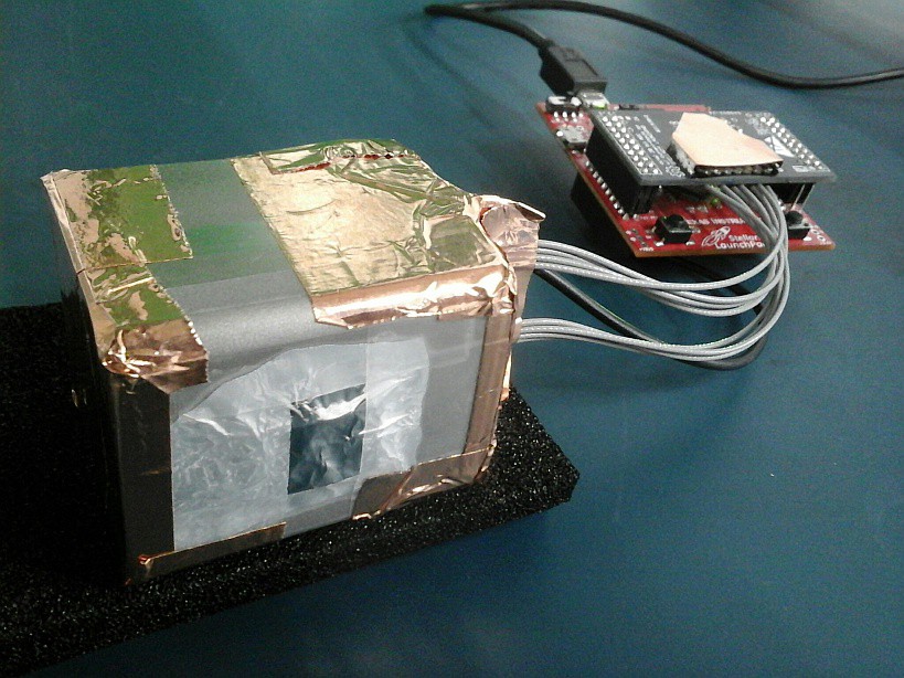
edit: Settings: 18kV, 110µA. Nice.
"I still have the parts for your DDC118 booster pack, do you have any assembly instructions?"
"throw that old PCB away"
Here's the new one. Guess I'll find out tomorrow that those u.fl connectors are spaced too closely or that the diff pairs have a polarity twist somewhere.
new minor revision:
- has proper footprints for U.FL connectors. They feel right for the job, right now I don't care much about the added capacitance due to coaxial cable
- tidies up passives
- actually spells out the channel numbers at the connectors and signal names near the pin headers ;-)
- removes LDO
- introduces differential DIN / DOUT
- introduces series termination resistors
- has 2x1 receptacle and 2x2 pin header for stacked daisychaining (first board has GND jumpers, all except for the base board omit R5/R6 in favor of a pair of wires that re-route DOUT/!DOUT, last board is unmodified (not pretty, but I couldn't be bothered to go 4-layer at this point
- introduces NC7SZ175 SC70-6 single UHS D-type flipflop which synchronizes CONV transitions to CLK_4X rising edge within < 5ns as per requirement (ds: sub-10ns for best performance), since I don't want to ensure these stay synchronized no matter what the Timer/Counter configuration I'll sync it in hardware. Will have to investigate beating anyway (+/- 0.5 clock cycles = 200-250ns w.r.t. 100µs-10ms integration time...)
- not yet given up on shields
- short circuits at the corners to avoid power-up when board is in wrong orientation (avoids killing the expensive IC)
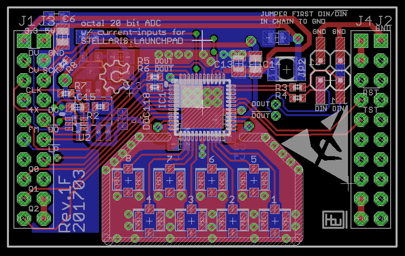
"todo":
- see if moving SPI clock (not in sync with converter) up past the REF3040 (U1) changed anything
- not too excited about those digital traces running across the reference buffer. DOUT/!DOUT now diff routed to cancel capacitively coupled possibly async (w.r.t. ADC clock) bitstream, async SPI clock trace relocated, rest of the signals are static
- build 2 new boards and use a full 16 pixel sensor. Oh boy...
____
edit: had a few hours of sleep, found mistakes and fixed them ;-)
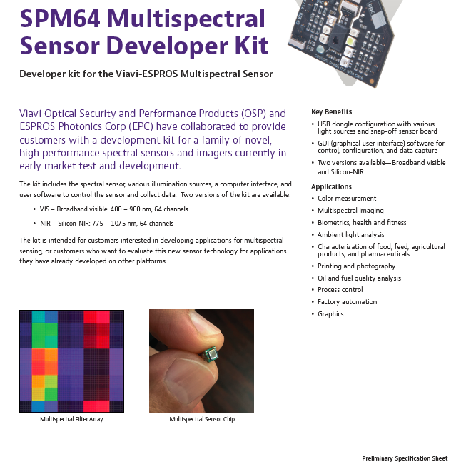
What's more important - achieving a goal or seeing a project through? You decide. ESPROS obviously managed to get a simple (diffraction based?) filter matrix slapped onto a camera sensor, making a cost effective and elegant device called Viavi.
Need UV A/B as well? Grab a VEML6075.
Meanwhile the Optical Inch will continue its journey with an LED array and Si PIN diodes for in-situ x-ray imaging. Stay tuned.
https://www.espros.com/photonics/spm64/
Create an account to leave a comment. Already have an account? Log In.
Become a member to follow this project and never miss any updates
 Dimitar
 Jarrett
 David Cook