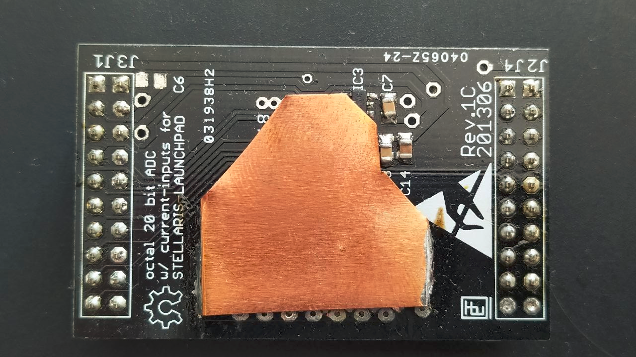
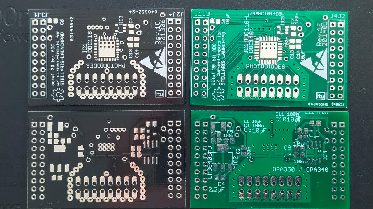
of 2 u.fl connectors added instead of 2.54mm pin headers.
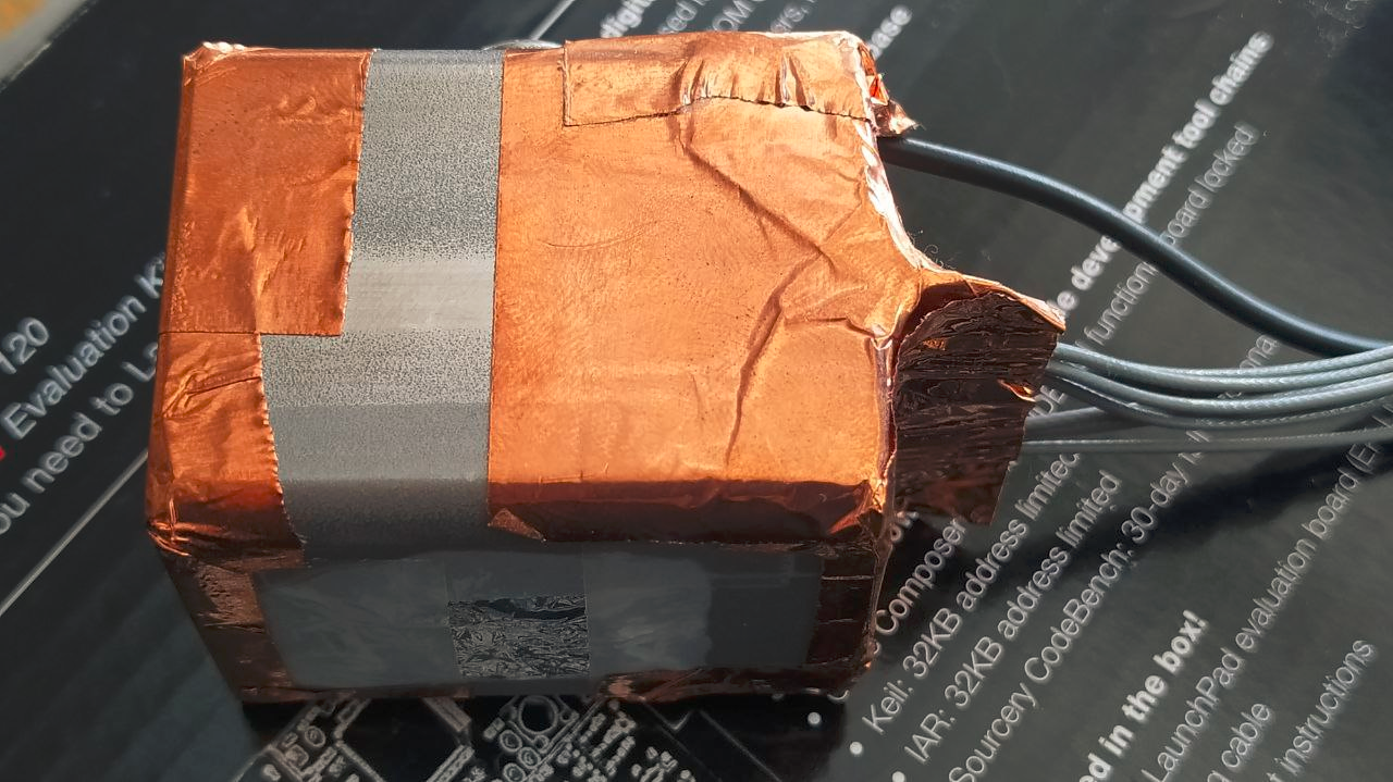
3 pin diode array with Pb aperture. Signal GND inside is left disconnected from the sensor head chassis GND and only connected on the DDC118 board.
4 An incomplete iteration - the LDO is still on Rev.1E. Attempts were made :)Should I have a need to build another board, it'll probably look very different today.
- u.fl connectors are okay for prototyping and even for photo diodes spread across a larger area, but it serves well to keep everything on the same PCB. Whether it's worth moving to shielded mezzanine connectors or not, remains to be seen.
- Common-mode noise isolation via digital isolators.
- separate board with JST XH or Molex KK 254 header..
- Common-mode filter in the power supply lines. Local 5.0V LDO. Optionally a low-noise isolated converter can be used (Ti SN650x + transformer).
- An array of DIP switches to short every input individually. Alternatively, the board could also be fitted with a flexprint connector to minimize the length of input traces / exposed conductor length. A folded piece of Cu tape, or a bit of Nickel foil can be inserted into the FFC header.
These ICs are highly susceptible to ESD damage, and separate protection diodes might invite unwanted leakage paths. For assembly, transportation and initial tests, all inputs should be connected to signal GND. DDC118 is rather expensive, so it's hard to imagine scenarios where it should be exposed to damage. - Source-side series termination resistors in the data lines could reduce any possible impacts of fast slopes.
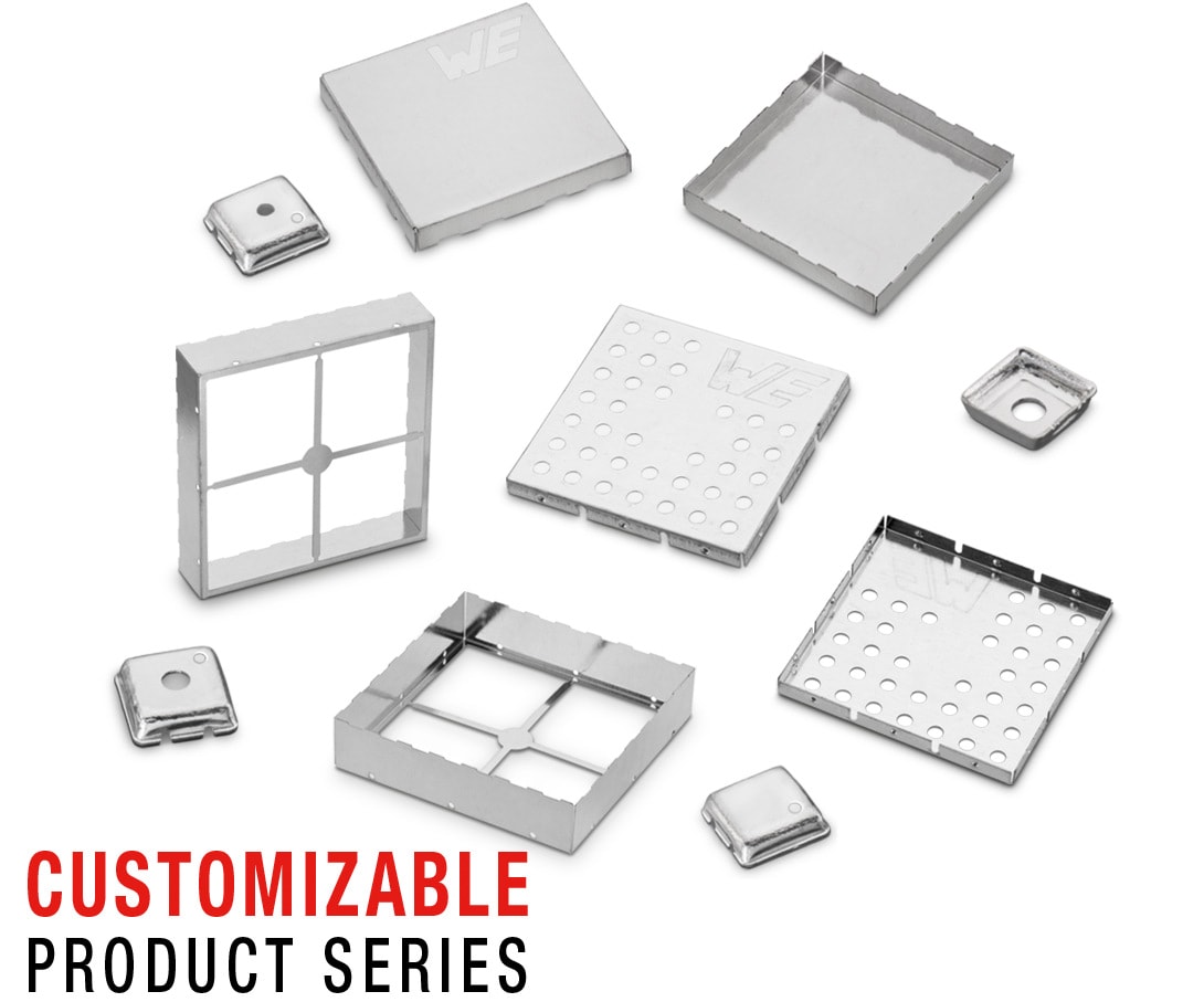
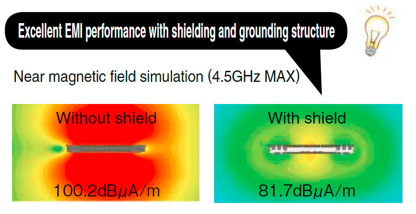
WE-SHC shielding components:
Hirose DF40GL shielded mezzanine connectors:
 helge
helge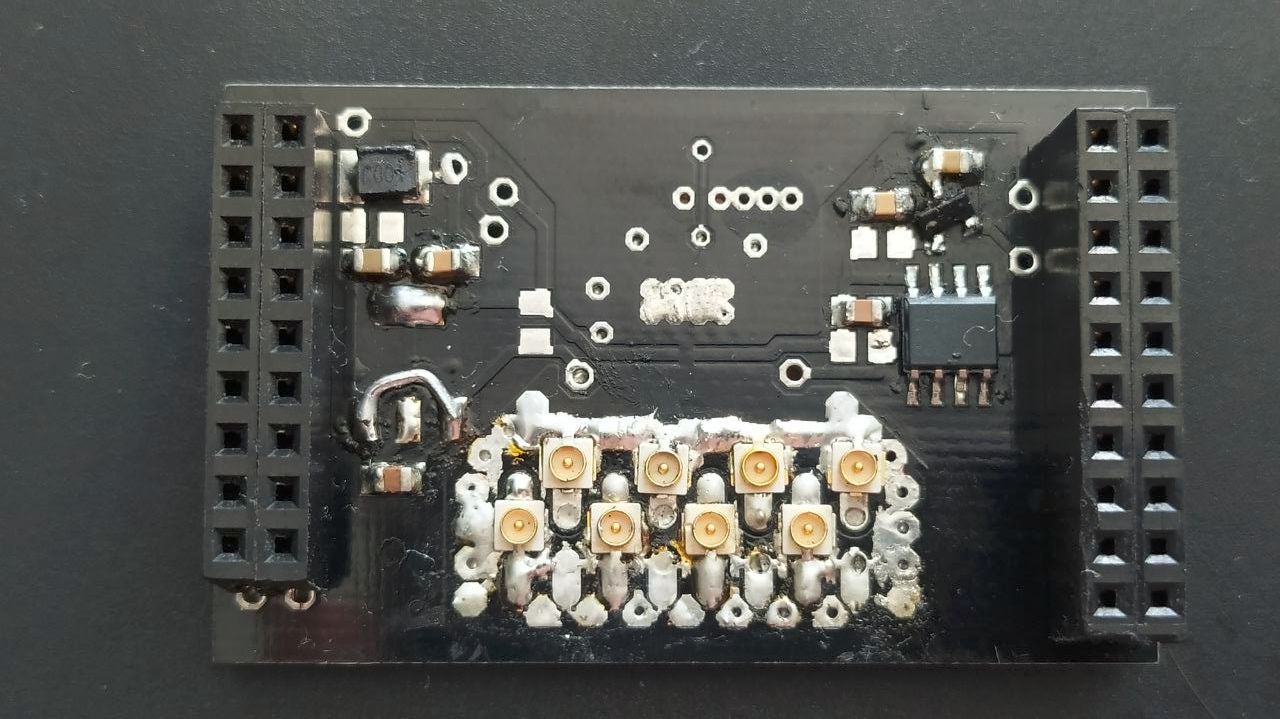
Discussions
Become a Hackaday.io Member
Create an account to leave a comment. Already have an account? Log In.