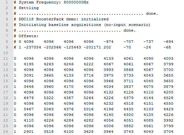
the DDC acquisition chips achieve 100% sampling time by alternating between two integration stages per channel identified by "Side A" and "Side B" for the two integration phases.
Now these integrators are not made equal, which causes different offsets and scaling factors to be applied to the acquisitions. I did find the offset issue somewhat disturbing so I addressed it first.
Let it also be noted that the CONV synchronous effect might also be in part due to LED activity or the CONV signal / trace itself. I remember it getting worse as the range is decreased.
Here we go:

unfortunately the first four data channels (mapped to input channels 1, 3, 5, 7) have some issues. I've contacted Ti to see if they have an idea and can help me out.
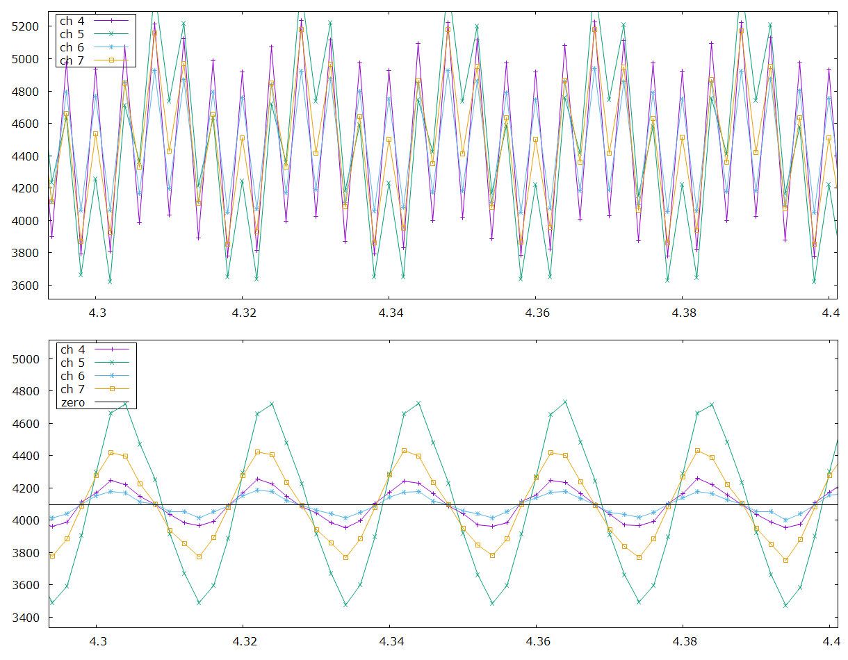
The remaining four channels however look quite promising, they still work quite well. For the DDC118 with 8 inputs there are 16 offsets to be kept track of. Here's what the output data looks like without (and below, with) Side A/B offset compensation:

this is 500 samples/sec, 350pC full scale and the board has just a bunch of 20cm long coaxial cables attached to the inputs.
I've also created a github repository and uploaded the demo code.
 helge
helge
Discussions
Become a Hackaday.io Member
Create an account to leave a comment. Already have an account? Log In.