 PN Labs
Its been a while since I updated this feed, so here it is with progress:
- Changed from DIP switches back to potentiometers for voltage adjustment - continuous adjustment is better for something as sensitive as voltage cutoffs
- Started designing a calibration jig that can measure the voltage cutoffs of each board. This is because when doing something as critical as undervoltage protection of lithium cells, having a typical 1-3% error in the voltage cutoff equation (as seen from internal testing of Protect modules) makes a difference in protecting the battery and the amount of energy that can be drawn before shutdown.
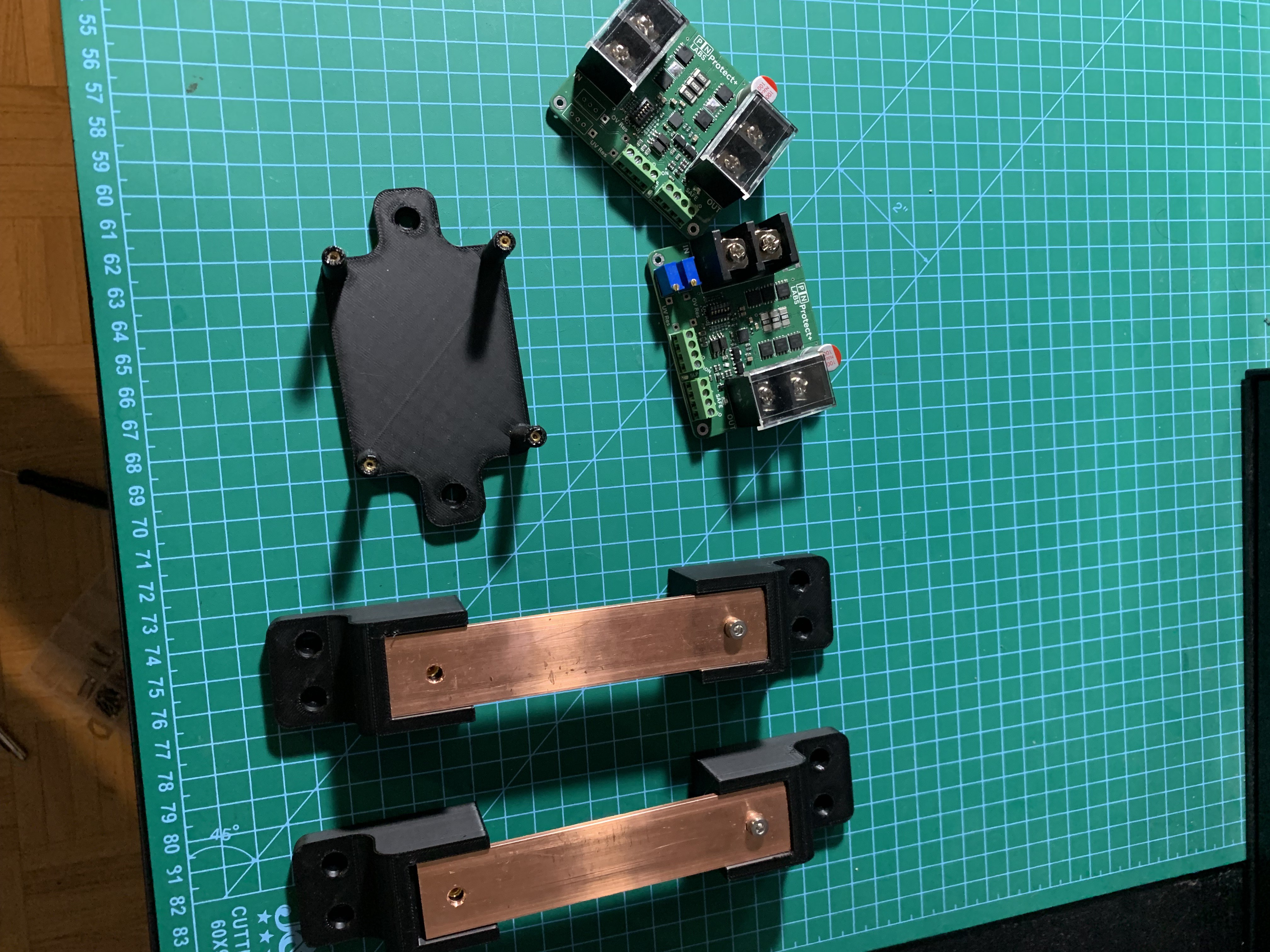
- First functional prototype has been received by PCBWay and hand assembled! A few differences I noticed when ordering compared to other board houses:
- PCBWay supports higher copper weights like 3 Oz, 4 Oz, and much higher, whereas other board houses like JLCPCB can only do 2 Oz currently. This is very important for high current designs (like the Protect+) where large copper pours (and stitching together different pours on different layers) are necessary to draw heat away from components on the board.
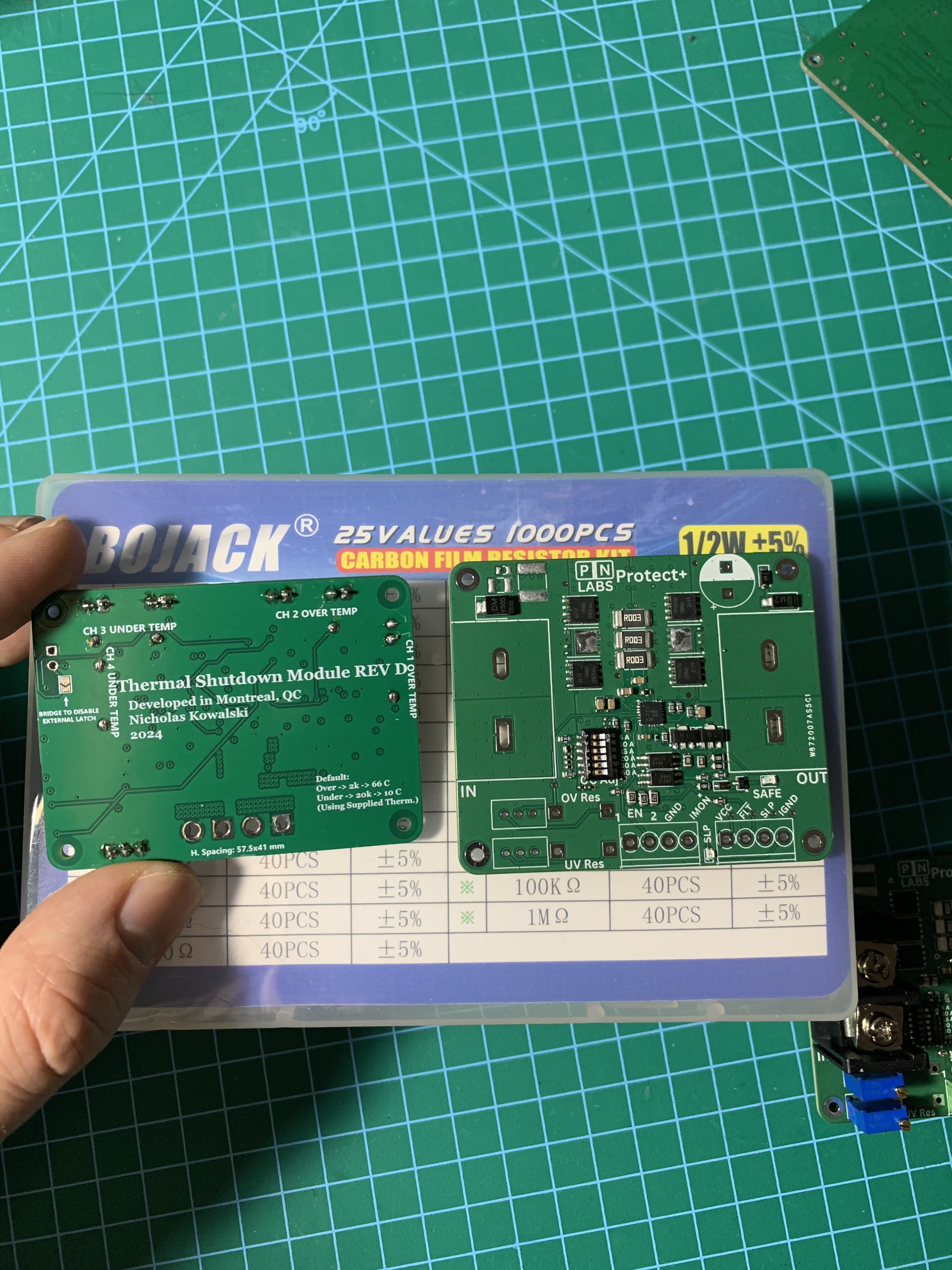
- I found the green solder mask on the PCBway boards to be much more visually appealing and higher quality than what I am used to. The dark olive color makes the board look very premium, and it reminds me of the PCBs you sometimes find in precision equipment with an ENIG finish. I've put a comparison between the Protect+ prototype and another board below.
- One mistake I made when ordering is not understanding the difference between the framework and non-framework stencil option. I think that the website pictures on the ordering page explaining the differences could be made more clear to show that Non-framework is the one most people hand prototyping would want (they should delete the confusing holes on the sides). I ordered the one with framework and it came separately, glued to a big aluminum frame which was great but somewhat unnecessary for my hand assembly.
The prototypes cutoff at the right voltages and everything seems to be in order, so the next step is to do some preliminary power testing to see how the board copes with in-rush current, plus its steady state thermal profile at different power levels (2 FETs or 3 in parallel?).
Discussions
Become a Hackaday.io Member
Create an account to leave a comment. Already have an account? Log In.