Design choices:
16-Bit RISC CPU.
Uses 7400 series logic chips.
Harvard architecture with separate EEPROM program memory, and data RAM.
Memory address space is 32K x 16 bits program, and 32K x 16 bits data.
Fits on a single PCB. State of registers can be displayed by LEDs.
To reduce chip count, uses universal ALU chips 74LS181.
One Accumulator 16 bit,
Program counter PC 16 bit,
and 16 logical registers.
----------------------------------------------------------------------------------------------------------------------------------------
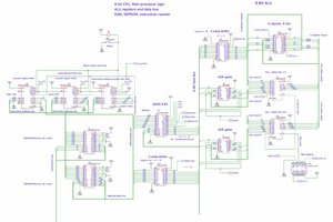
Computer consists of five main subsystems, as shown on schematics:
Program EEPROM 32k x 16 bits, and Program counter,
Instruction decoder and control logic,
555 Clock timer, and I/O ports,
Static RAM, 32k x 16 bits.
The universal 16-bits ALU, and 16-bits accumulator register.
----------------------------------------------------------------------------------------------------------------------------------------
Principle of operation:
All instructions execute in 1 cycle. This simplifies CPU control logic.
The processor uses simple 2 phases clock:
On positive edge of the clock (0 to 1), instructions executed.
On negative edge of the clock (1 to 0), the program counter incremented.
The 555 timer generates clock signal CLK, adjustable from about 1 Hz to 1000 Hz. But the
computer itself is capable of much higher clock rate, probably up to 1 MHz.
The program counter is incremented on the negative edge of the clock (inv. CLK). It resets to 0,
when "reset" button is pressed.
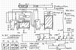
When ‘inv. Load Addr’ signal it low, the address counter loads next address from the address/data bus, i.e. it executes Jump instruction.
The instruction address goes to the address inputs of the 32k EEPROM.
The outputs of the EEPROM drive the instruction decoder and CPU control logic
The 74LS181 ALU chips used for arithmetic and logic.
Two 8-bit flip-flops used for Accumulator.
Two 32k SRAM chips used for data.
Registers are logically mapped to first 16 addresses in RAM.
I.e. physically it has only two registers, Accumulator and PC.
32Kb instructions and data address space,
----------------------------------------------------------------------------------------------------------------------------------------
Instruction set is minimal, with the idea of RISC,
but allows to execute complex programs.
The instructions and data are 16 bits.
Instruction format is: 6 bits opcode, 10 bits for address/data.
Instruction types:
Arithmetic instruction
RR Acc, register
Arithmetic operation with Accumulator and one register.
Here Acc is accumulator, register is one of the 16 registers.
Arithmetic instructions have special format:
6 bits opcode, 6 bits encode arithmetic instruction, 4 bits encode register.
Arithmetic instructions RR include all of the following:
Add, Subtract, And, Or, Xor, Not, Shift left, and more.
Any operation supported by 181 ALU chip can be used.
Load Acc, mem
loads data from memory to Accumulator
Store mem, Acc
stores data from Accumulator to memory
Load Acc, immediate,
loads immediate value to Accumulator
Jump address
jump unconditional to address
JC address
jump when carry bit (conditional jump)
In port
input from port to accumulator
Out port
output from Accumulator to port
* Notes:
arithmetic operations only execute between operands
in Accumulator and one of the 16 bits registers.
The instruction has only 10 bits for address/data,
But the address value is extended to 16 bits, by combining it
with 6 bits from High Address bits register.
Program EEPROM and data SRAM have separate address spaces, 32k each.
16 registers are mapped to the first 16 addresses in SRAM. That simplifies the design.
I.e. storing value to first 16 words in memory is same as storing it to...
 zpekic
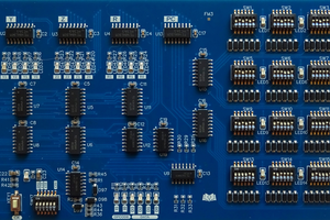
 AranweLTT