 electronicsworkshops
Introduction
In this project, we design and implement a DSP-controlled inverter circuit using the LaunchXL F28379D development board. This project demonstrates how a high-performance digital controller can be used to generate precise PWM signals, control switching devices, and achieve efficient DC-to-AC conversion.
For Full Project:
https://electronicsworkshops.com/inverter-circuit-using-launchxl-f28379d/

This project is ideal for:
- Power electronics learners
- EV and motor control engineers
- Students working on DSP-based inverter projects
- Researchers exploring real-time control using TI C2000 controllers
What Is an Inverter?
An inverter is an electronic circuit that converts direct current (DC) into alternating current (AC) at a desired voltage and frequency.
Common Applications of Inverters
An inverter is an electronic circuit that converts direct current (DC) into alternating current (AC) at a desired voltage and frequency.
Common Applications of Inverters
Electric vehicle traction inverters Solar power systems UPS and backup power systems Variable frequency drives (VFDs) Industrial motor control
Why Use LaunchXL F28379D for Inverter Design?

The LaunchXL F28379D is based on Texas Instruments’ C2000 Delfino™ DSP, which is specifically designed for real-time control applications such as inverters, converters, and motor drives.
Key Advantages
- Dual-core CPU (CPU1 + CPU2)
- High-resolution PWM (HRPWM)
- Fast ADCs for voltage and current sensing
- Real-time control capability
- Excellent support for motor control and power electronics
Because of these features, the F28379D is widely used in EV inverters, onboard chargers, and industrial drives.
Gate Driver and Signal Conditioning Circuit Explanation
This circuit represents the gate driver and PWM signal conditioning stage of the inverter. Its main role is to safely convert low-voltage PWM signals from the LaunchXL F28379D into high-current, high-voltage gate drive signals required to control the inverter power switches (IGBTs or MOSFETs).
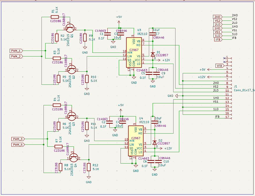

This circuit is the gate driver stage of the inverter, used to interface the LaunchXL F28379D DSP with the inverter power switches (MOSFETs or IGBTs).
The PWM signals (PWM_1 to PWM_4) generated by the F28379D are first passed through transistor-based signal conditioning. This stage improves noise immunity, provides buffering, and protects the DSP from the high-power section.
The conditioned PWM signals are then fed into the IR2110 gate driver ICs. Each IR2110 drives one inverter leg by providing:
- High-side gate drive (HO)
- Low-side gate drive (LO)
A bootstrap circuit (diode and capacitor) is used to generate the floating supply required for high-side switching. This allows the high-side MOSFET/IGBT to turn ON even when its source/emitter is at high voltage.
The circuit operates with +5 V logic supply and +12 V gate drive supply, with proper decoupling capacitors to ensure stable and reliable operation.
Finally, all gate outputs and feedback signals are routed through a connector to the inverter power stage, making the design modular and easy to integrate.
Inverter Power Stage and Output Section
This circuit represents the power conversion stage of the inverter, where the DC input is converted into AC power and delivered to the load through a transformer.
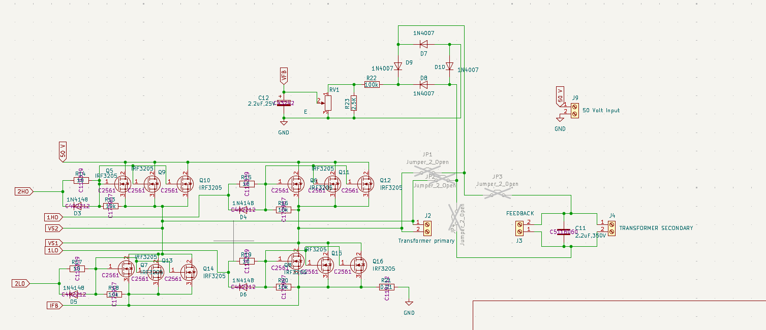

The inverter is built using IRF3205 MOSFETs arranged in a full-bridge configuration. These MOSFETs are driven by the gate driver circuit (IR2110), receiving high-side and low-side control signals (1HO, 1LO, 2HO, 2LO) generated by the LaunchXL F28379D.
When the MOSFETs switch alternately according to the SPWM signals, the DC input is converted into a high-frequency AC waveform at the transformer primary. The fast switching diodes (1N4148) protect the gates from voltage spikes, while gate resistors control switching speed and reduce ringing.
The transformer provides:
- Voltage level conversion
- Electrical isolation ...
 kamalkedin123
 Osman Mazinov
 engineerkid1