-
Layout and Alternate Version
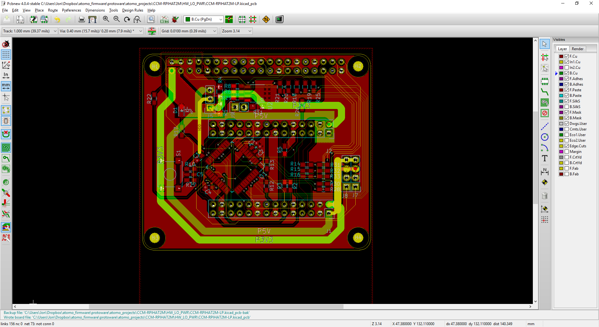
04/04/2017 at 10:08 • 0 commentsOK, looks like we are done here, at least for the core layout work. The boards still need some additional graphics, but everything else is pretty well ready to roll.
We've got two versions, one with the 34-pin connector for the Power module and the other only has 3.3V and 5V on board. The low power version does not have the additional components needed to protect the Pi for powering the 5V from the board if there is a power conflict when the USB is plugged in.
Next up, do some quick graphics, send the boards out for production, and post up the files and a writeup for the project.
-
Final Schematic
04/03/2017 at 04:18 • 0 comments![]()
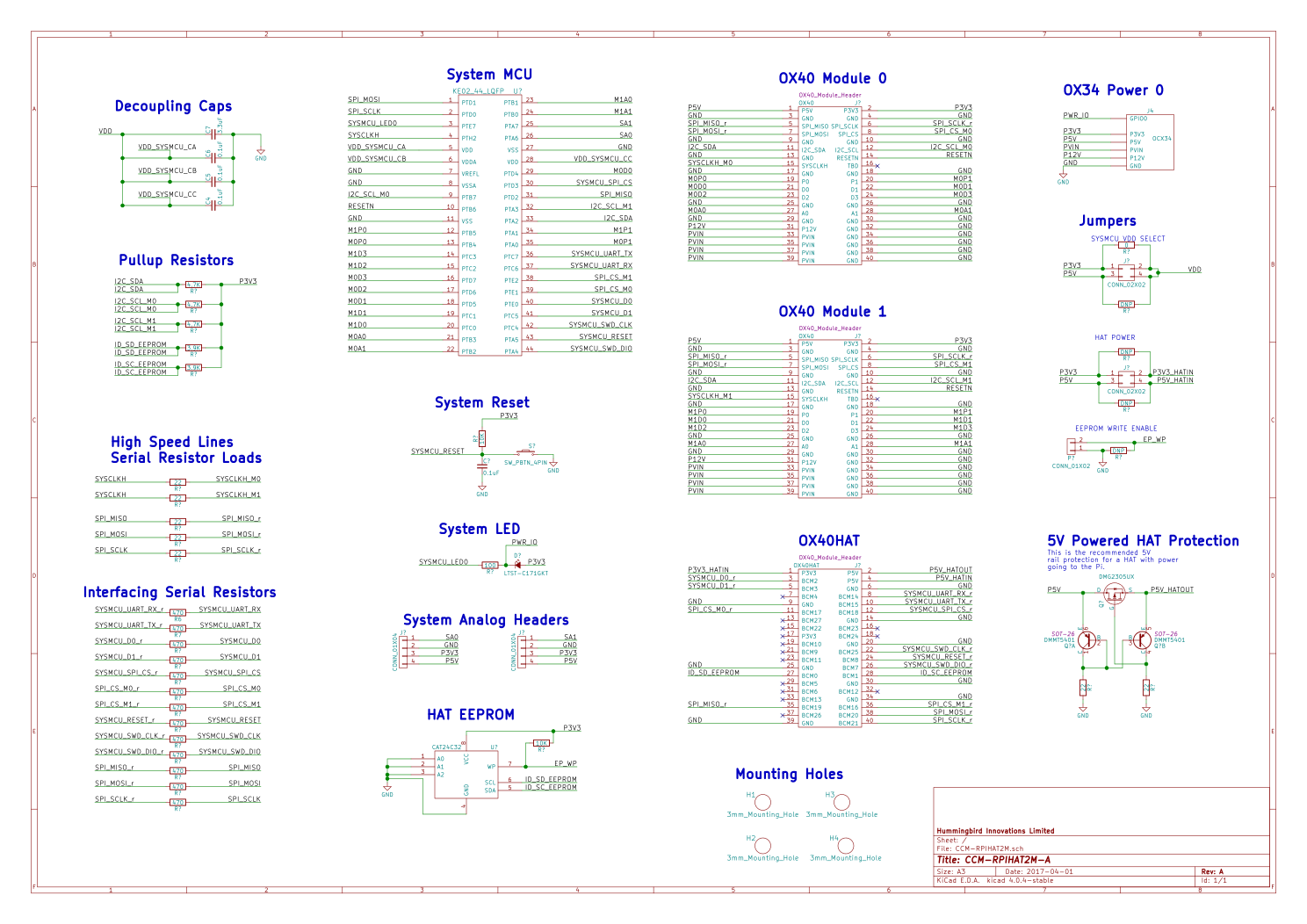
And this is the end result schematic. Some notes on how things turned out:
- In the jumpers section, you can see that there are DNP or 0 Ohm resistors used in parallel to a pin header. This will give users a choice of either using jumpers with a pin header or to solder their choice without pin headers. All of these except for the one 0 Ohm resistor will be unpopulated to start with.
- We are assuming that if the user is using the system as a powered system, the 5V and 3.3V power is coming from the HAT for the board. This means that to program the system MCU, power will need to be applied to the Power header (at least 3.3V) or the user will need to configure the power jumpers to run the HAT off of the Pi power.
- If the power from the Pi is enabled, it is up to the user to NOT connect those supplies to the Power header. It is possible to cause a power conflict if this is enabled and burn out things. It would be possible to run 3.3V and 5V from the Pi with 12V and VIN coming from the Power header. Everything should be OK as long as there isn't a conflict with the grounds.
- I'm trying a new way to define the decoupling caps. I don't like the way that they are traditionally banked together without a good reference to where they should be placed on a board. The way they are done here *should* give feedback on the layout which caps belong to which pins. These ideally are placed close to each pin they supply.
So, I don't have a final BOM created yet for this, but I'm guessing around $3-3.50 in quantity. This would make it suitable for something around a $12-15 retail. I need to see what the non-powered version clocks in at, but I think we can shoot for that as a $10 retail price.
Next is to select the footprints and then do the PCB layout. The first step will be to put the parts on the board and import the board layout from the 3D model for placement of connectors.
-
Dualism
04/02/2017 at 11:09 • 0 commentsI've been working through the schematic and adding the final bits before going to the PCB layout. One feature that I forgot to factor into costing so far was the parts for preventing a power conflict if our board is powered and the Pi also is powered from a USB source at the same time. The HAT spec does have a solution for this. In our case, we want to be able to either power the board from the Power module or from the Pi (ideally), so we need to take that recommended spec and tweak it a bit.
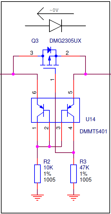
Looking at just preventing a power conflict on the 5V, which is the original HAT spec design, it uses one P-Channel MOSFET plus a matched PNP transistor pair.
![]()
This would work if we only are thinking about powering the Pi via 5V from our HAT. We have another condition of powering our board from the Pi, at least the 5V and 3.3V. Looking at using a switch to bridge the power, options with enough current handling capacity are quite expensive. It seems like the best option is to do a single set of jumpers between the Pi and the HAT on one 5V and one 3.3V pin. This will be normally unpopulated, and will need to be well labeled to prevent accidental usage.
On that note, the extra components involved probably end up breaking the cost limit that we need to hit with this design, but it does open a simple option. We will do two designs, one that has the Power module and the other without. This allows for a lower cost for the unpowered version, and we might be able to fit in a higher spec controller or something like that. Dropping the VIN power means that we can use the 28-pin version of the IO module connectors, which also reduces the cost. To maintain the compatibility with the HAT spec, we will still need to keep the full 40-pin connector to the Pi, so that will drive the overall size limit we can have.
-
From Spreadsheet to Schematic
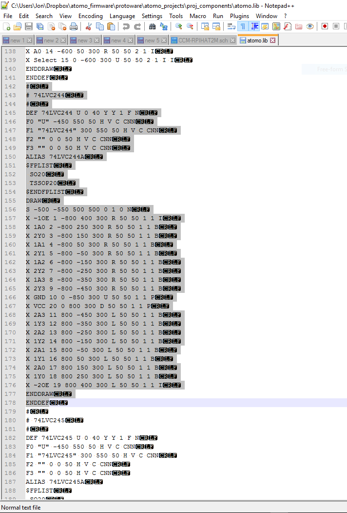
04/01/2017 at 13:41 • 0 commentsIn the last post, I linked to my system design spreadsheet. If you look, that has a bunch of stuff on it that is kind of random text strings. Those are used for importing the configuration into KiCAD without too much hassle. The components are driven by this definition and the net connections are also handled using this. Obviously, this is a big hack. My process is to create a component in the KiCAD component manager interface, and then update it with the pin configuration from the spreadsheets. That requires opening the component library in a text editor, finding the component definition, and then swapping out or inserting the pin definitions. After doing this, you need to open KiCAD fresh to get the changes. If you have it open while editing these files, you either will need to not save or just re-paste the updated info if you do.
This is a component file. The section highlighted is a single component definition. The lines that start with X after it says DRAW are the pins. All that I do is create a list of pins with appropriate locations and insert them after any drawing entities, before the ENDDRAW line.
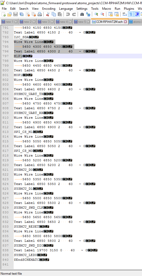
This is a KiCAD schematic file. It is a bit more free-form than the component file. If you look through it, it has component placement and definitions for wires and text labels for Nets, among other things. The easiest way to update this file with wires and nets is to delete the existing ones from within the schematic view in KiCAD (if any), save, and then open it in a text editor. If you scroll to the end of the file, you will find the EndSCHEMATC line. Insert your new stuff just above that line. Be careful to not break up multi-line items, otherwise it will cause an error and nothing will load after the error point in a file. I've highlighted a wire plus net text label for your reference. That is pretty much it. You could update the spreadsheet to match the exact coordinates on the spreadsheet, but I find it easy enough to move it once it is in, and you should give it a once-over anyhow.
You might wonder if it is worth the trouble. I found with systems that have common design features or just very complex ones with high pin counts along with multiplexed features on pins, something like this is really needed to keep track and not have small errors that are very hard to spot in complex designs.
The next step is to finish the schematic in KiCAD, iterate the pin and net configuration, and then move it into the PCB Layout.
-
Configuration Spreadsheet.
04/01/2017 at 13:16 • 0 commentsThis is how I design systems, at least at the moment. For me, the hardest part of creating a system design with things like MCUs where there are multiple functions for each pin. You have sometimes six or seven different options and many times there are other connected interdependencies for using one particular function. Pin configuration for an MCU can be done (sometimes) with tools provided by a vendor, but that doesn't really help much with overall system design. Things like assigning consecutive bits on a port to consecutive pins is important, but it gets complicated quickly when doing systems with more IO involved.
So, what I do is map out all the major pins that need to be connected, start assigning those functions that are most limited availability, and then rinse and repeat until all connections are made. Yes, you *could* do this in the schematic, but how do you verify that you haven't used a given function already or duplicated a net name? On more simple designs, this is overkill, but even this one benefits from this approach.
OK, what was the outcome of the configuration? What were the tradeoffs to stay within our target? One item was I2C. Ideally, I would put some sort of multiplexing on the I2C bus so that each IO module gets a separate interface to the bus. This allows using more than one of a sensor that has a fixed address. One on each IO module. Well, the MCU only has one I2C bus, it is a lower pin count part. *But*, it does have two different I2C implementations for the same bus. This means that two pins can be configured to be I2C_SCL. So, what I've done is used both of those pins and only connected them directly to each IO module. This should allow for me to reassign the functionality and address each IO module as needed. Yes, there is setup and teardown to do, so there is some overhead. This isn't too different from a separate I2C multiplexing IC addressed on I2C.
What other considerations were there? SPI, it looks like we should be OK, if the Pi is in place and is interfacing via SPI, it will be the master, otherwise, the KE02 will be the master. Faced with the limitation of a 44-pin KE02, I started with connecting between the IO modules first, and then used what was left over to interface as much directly to the Pi. The result is not a 100% pin coverage between the IO module pins. Instead, we have UART TX/RX, SWD + Reset, and two additional GPIO pins connected between the Pi and the KE02. This allows for options on how to send data back and forth, plus either interrupt lines or possibly a parallel data interface. The SWD + Reset gives us a direct way to program and debug the KE02 via OpenOCD on the Pi.
Most likely, the KE02 could either run a generic interface program with configuration and data is sent via SPI or UART or it could be programmed with specific behavior and then either run independent of the Pi (a lightweight stand-alone app) or be able to interface on any of the connections. Technically, you could even use SWD to do some direct memory polling or something like that, but I don't know how practical that is.
That is the core system design, next up is the schematic layout and then PCB layout.
-
3D Model and Final Design Decisions
04/01/2017 at 09:08 • 0 commentsThe first 3D model of the RPi HAT module helped to solidify the overall design approach.
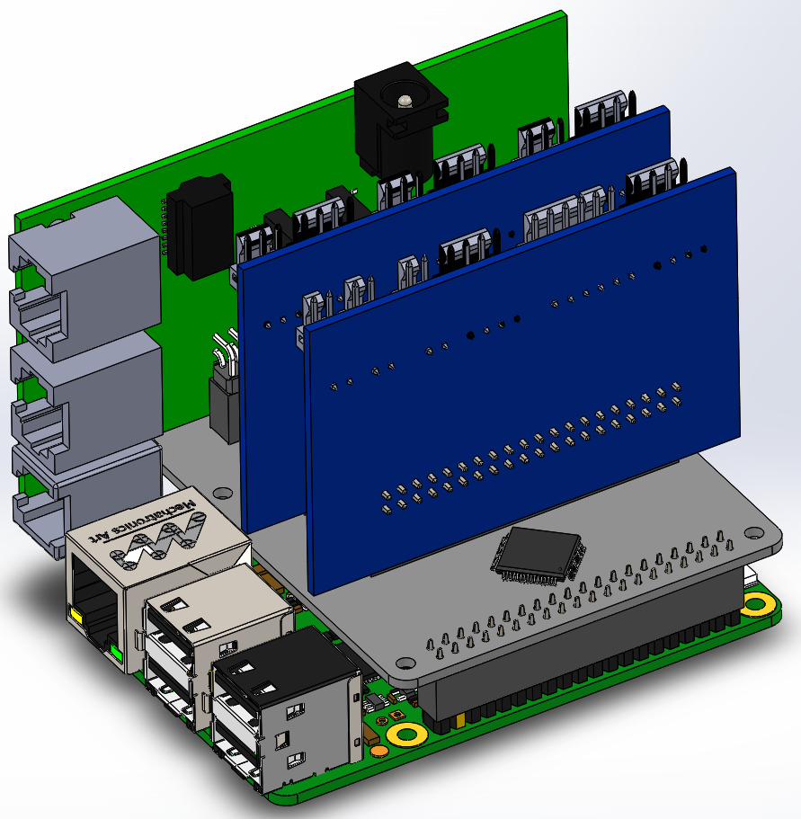
What you can see here are two standard powered (40-pin) IO modules and in the back is a POE Power module. This is a good configuration to design around because the POE module extends down below the plane of the Connector module and has the network jacks at the same face as the Raspberry Pi. So, going with this constraint, I've placed the Power module at a reasonable distance from the Pi connectors and set that position. Another option would have been to place the power on the other side, above the HAT connector. That would have resulted in the POE connectors on the other side than the Pi connectors and it also makes the power routing not possible with a standard HAT board footprint.
On the other hand, this layout is close to the existing Connector modules, so the layout work done for those will be a good reference.
I've placed the two modules at a spacing of 0.7 inches (2.54mm*7) to allow for standard proto board to be used to build a combined 2 IO module board, and the power is at 0.8 inches (2.54mm*8) for that same reason. This results in the layout shown (when combined with the constraint of keeping the power connectors clear of the Pi connectors).
Now, that fully constrains the interfaces of our design, and gives us a PCB with placement of all connectors. The next step is to then look at what MCU to embed in the design. Shown in the 3D model is a 64-pin LQFP, which is about the largest component we could practically put in. But, we need to consider cost and functionality to make some tough design decisions.
The biggest constraints to consider are wanting a more robust MCU for both helping to isolate the Pi but to also make this a good starter board for people with Atomo. Given my current experience with NXP Kinetis line ARM based MCUs, the only option there is the KE line. Of those parts, the KE02 line is the least expensive, with parts available in the $1 USD range. The KE04 line is similar, but it has been designed to complement the KE02 line so it has a smaller part and then larger parts, but the KE02 line for 44-pin components is a pretty sweet spot for the number of pins and all other requirements. The 40MHz version starts with just 16KB of flash and 2KB of RAM, but that should be OK for very basic applications or setting this up as an IO expander for the Pi.
Moving up to a 64-pin package also comes with more memory, so the step up is about $0.40 USD. Since the other constraint for the design is to try to fit it into a $2.50 BOM cost, that $0.40 is going to come at either a cost of increasing the retail price or sacrificing something else, if there is anything else to sacrifice. Assuming the basic costs are:
ITEM QTY Cost Total PCB 1 0.7 0.7 MCU 1 1.08 1.08 Connectors 4 0.15 0.60 Misc 1 0.2 0.20 Total $2.58 We can probably just get the design into our target with a 44-pin component. Otherwise, we will need to step up the retail price.
So, the next question is what can you functionally do with that 44-pin part? That will be the next log entry.
-
Design Decisions
03/29/2017 at 06:22 • 1 commentThe last few days have been looking at the pin configuration of a system that ran the Pi pins directly to a module header with analog pins provided by an MCU. Not that the whole time was spent on this, but more doing some planning and then digesting the limitations of different options. It ended up to do a 4-module design, it would need a 64-pin package MCU to provide all the support (2 modules completely on the MCU and support for the other 2 modules that are mostly handled by the Pi). This starts pushing up the complexity of the design and also the cost of it, somewhere that is outside of the ideal solution space.
So, I stepped back and considered what are the design goals. One option is to go for a 4-module design but to limit it when connected to existing connector boards (remove system pins, etc.). The problem with this is implementing a non-standard pinout of the modular controller connector kind of defeats the purpose of having a standard. The other option was to re-assess the benefits of hooking up the Pi to a system like this and see if there was some design in the middle that really put some benefits back into it over just the existing controller modules.
The current (final) design direction for this project is this:
- Create a 2-IO Module compatible design that is a Raspberry Pi HAT.
- Instead of creating an adapter module that works as a controller module, create a combined controller-connector module that integrates an MCU that acts both as an intelligent buffer between the Pi and the IO modules as well as extends the Pi with ADC and other facilities.
- Keep the total retail pricing at $10, which means we want a BOM cost of something like $2.5.
- Use a 5V and ESD tolerant part, like the KE series to protect the Pi from things that would normally damage it.
- Create a powered and unpowered variant.
- Make sure it is compatible with extended modules, like the POE power module, since, well, that fits really well with the Pi as a network powered installation.
Now that the design is more at a system level, it is not as important to do the pin connections first, but to look at the board level configuration. I've started with creating a full HAT sized board and put an assembly together that has the features required to look at spacing of things and to consider the overall use case. That gives us a direction to help define the system inputs and outputs which then defines the requirements of things like the MCU. OK, time to go hash that out.
-
Design and Project Decisions
03/22/2017 at 07:31 • 0 commentsYesterday set up this project and filled in info to get it up to where I was at. Today started fleshing in the design decisions to get things moving further. After writing up a bunch of info for the Details Section, I think I'll use this log section for my design details and keep the high level project details to be more about the implementation of those decisions.
1st Design Decision: How to implement ADC pins?
So, after sorting out that the max of directly driven IO pins is two IO modules, I started looking at the overall design and usability and considered three options that I needed to research:
- Use an ADC IC to implement just the four ADC pins for a two IO module controller adapter.
- Use an MCU to implement all outstanding pins, including system pins and IO module ADC pins for a two module system.
- Use a slightly larger MCU to implement both all the needed pins for a two module system as well as act as an IO extender to make the controller adapter design work with up to a four IO module system.
Coming at things from a consumer product background. On one hand, I optimize for cost, and if that was the only consideration, the most obvious solution for the above would be to use a cheap 8-bit controller to do either option 2 or 3. However, even though the cost could be closer to $0.30 USD for the controller, this would be not as accessible for most of the other users for the system who are going to be programming ARM Cortex based controllers. So, 8-bit is not really an optimal solution because it is too different from other bits of the system, and this adapter is more likely to be hacked by end users in interesting ways.
The ADC IC would be easier to implement, but they cost about twice what even a full-featured MCU does for the same application. So, option 1 is out, unless you need specific things like paired analog readings on all pins. A fast and cheap MCU should be able to make samples and optionally do things like averaging or interrupt exceptions when a limit is hit. The basic features of reading ADC and then making it accessible via SPI or another route *should* not be too involved.
I've been using mostly NXP Kinetis line ARM based MCUs for most of my stuff lately. They are pretty easy to source, and have good options for development tools. The STM parts would also be a consideration, they tend to be either cheaper or have better specs for similar pricing. In this case, what bubbled up are two options:
- Two module design with the Pi providing all GPIO and bus connections, only provide the ADC for the two modules via a MKE04Z8VTG4
- Four module design using a MKE02Z16VLC4 to support all ADC plus two modules of GPIO and PWM.
The second option would be a little more expensive, the MCU is about $1 in reasonable quantities where the first option is about $0.6. But, once this is added into the cost of the overall adapter module, it would be a significantly better amount of functionality at what ends up being less than extra $2 on a retail price. The other part is that the HAT board size is larger than the two module controller board, so in order to get the full 40 pins on the HAT, plus mounting holes, we will already have enough room for the four module card edge connector (PCIe type 98-pin connector).
So, we will be designing a HAT that has a 32-pin ARM Cortex m0 as an IO expander and that uses the Raspberry Pi pins for GPIO/PWM functions on two Atomo IO modules plus another two IO module support using the IO expander. With the design of the Atomo controller interface, we either need to put the Pi direct module connections on the first two or last two, and that will define how this can be used with or without a Pi connected.
2nd Design Decision: Pi connects to modules 0 & 1 or 2 & 3?
This one has a few different tradeoffs:
- If we put the Pi controlling the first two modules, then if we use it in a two-module setup, the system really needs the Pi to work. Only ADC pins would be available without a Pi connected.
- If we put the Pi controlling the last two modules, then if we use it in a two-module setup, then we could program the expansion MCU to work without having a RPi there, but to access the Pi GPIO pins, you would have to use a four-module connector board.
With decisions like this, there are not always clear answers. On one hand, if this is a Raspberry Pi adapter first, it would make sense to give priority to having the RPi pins available in all common use cases. But, if we look at this now as a dual function board of a low-cost controller module plus support for direct Raspberry Pi HAT functionality, it would make just as much sense to prioritize the usage without the Pi installed. Since in both cases, the Pi would be connected to I2C and SPI as well as being able to control the other pins, it is probably better to make it function without the Pi on the two-module connector setup. From a functionality standpoint, there is less tradeoff this way, and it would make it more useful as a standalone module at the same time.
OK, so I need to reassign the module pins and look at how the expansion MCU needs to be included in everything to make the best of it.
-
Base Research and Initial System Design
03/21/2017 at 08:55 • 0 commentsYesterday I just researched the HAT spec to understand what all is required for compatibility other than just using the pins. I then started sketching out some solutions in spreadsheets to get a feel for how the available pins might work with the Atomo Controller Module interfaces. The plan is to use something for giving the ADC capability over SPI, since the Pi doesn't have ADC.
After looking at the ADC ICs and available MCUs, the MCU direction makes a lot more sense. It is significantly cheaper and is more flexible. There are two options that make sense:- Two module design with the Pi providing all GPIO and bus connections, only provide the ADC for the two modules via a MKE04Z8VTG4
- Four module design using a MKE02Z16VLC4 to support all ADC plus two modules of GPIO and PWM.
Either way, need to sort out the easiest way to communicate using what pins are available and not interfere with the current backplane design for multiplexed SPI selects.
Designing a Raspberry Pi HAT
How to design your own HAT module including ID EEPROM.
 Jon Buford