Capt. Flatus O'Flaherty ☠
-
All Rx Components now Working!
10/13/2017 at 11:41 • 0 commentsThe issues getting all the amp chips to work together has been solved - turns out it was a combination of bad soldering and one tiny trace on the LNA circuit being missing. The previous log showed a board design with small 0.2mm positioning pads - boards were manufactured with these features and proved to be incredibly effective in getting the chip exactly positioned. The chip does not seem to obey the laws of surface tension, which usually 'pulls' the chip into position
The effectiveness of the design is given by the uploading and downloading speeds of the cell phone and in the last test, with all the components working as they should do, uploading was at 2 Mb/sec and downloading was at 12 Mb/sec with a theoretical maximum of about 7 Mb/sec and 38 Mb/sec, which suggests that there is still some fine tuning to be done at some time in the future. Nonetheless, using this device inside a building improved the upload speeds by a factor of 2x and the download speeds of about 10x.
Just a quick note about 4G speed testing - The cell phone and the network communicate systems data with each other in both directions and the network will transmit actual useful data to the phone in increasing degrees of complexity depending on the signal quality that the phone receives. If the phone detects poor signal quality it will tell the network to give it data in a simplified format which in turn means that download / upload speeds are diminished.
The next step in the project would be to analyse the circuit with a Vector Network Analyser (VNA) to fine tune it and make sure that signal is not reflected back into the Rx antenna on the Rx side of the circuit. Another idea would be to upgrade the PCB stack to a better grade of material which would improve parasitic capacitance.
At some time it would also be nice to be able to get the Tx part of the circuit working but currently I can't test this without my network's permission.
-
Soldering Problems
09/19/2017 at 11:52 • 6 commentsAfter several weeks of trying to solder the RF amplifier chips I eventually concluded that the techniques that I was using to accurately position the chips was not up to scratch. I tried microscopes, magnifying glasses, magnifed eyeglasses that you jam into your eye socket - all to no avail.
Using the square drawn on the silkscreen was hopeless as the board manufacturer could, or would, not print the silkscreen accurately and this route proved to be a dead end.
I did elongate the PCB pads slightly so that they were visible, but the pads on the chips themselves are not visible at all so there was no possibility of lining them up at all - another dead end.
After a while, just by chance, I was able to get the two chips, the LNA and VGA working together by connecting up different boards and when they worked, they worked really well. This was nice as it effectively ruled out any incompatibility issues. Unfortunately, the laws of probability did not allow me to get the two chips working on the same board ..... Not yet anyway.
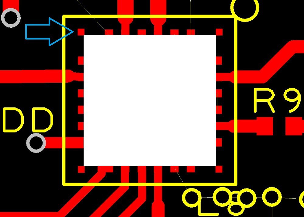
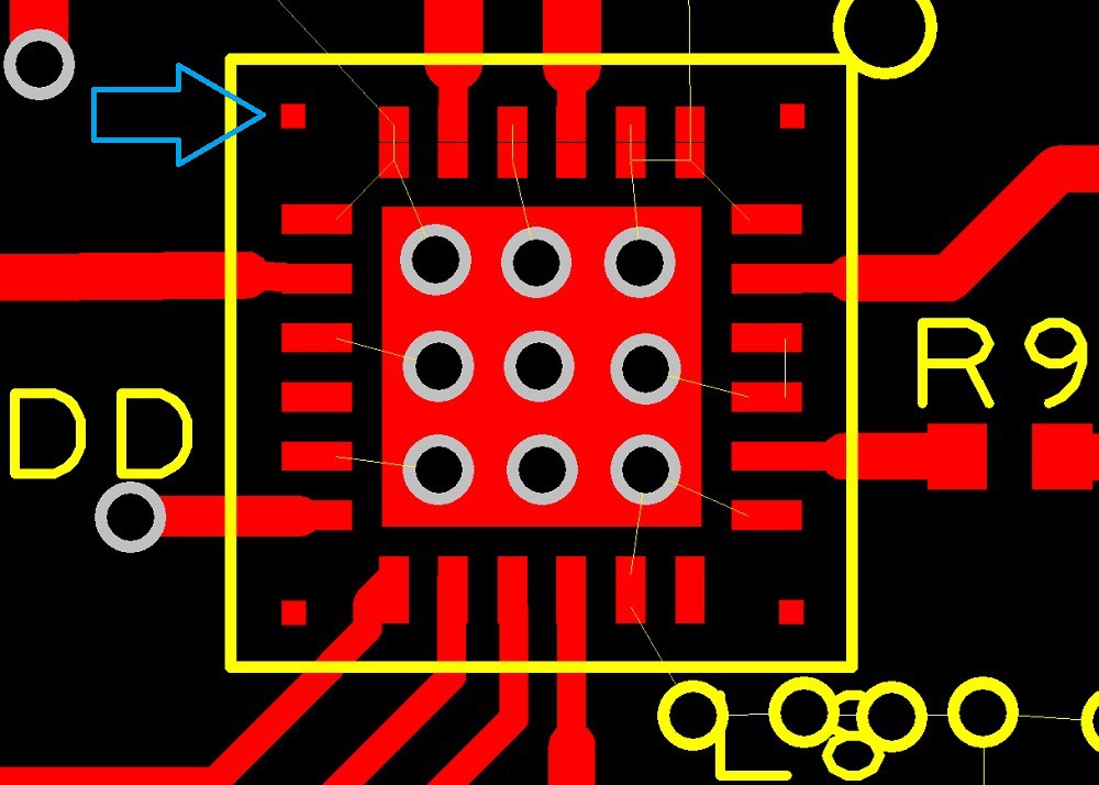
So, I needed a fool proof way of aligning the chips and eventually came up with the idea of using some top layer pads as markers instead of being used for electrical connections. In the diagram below there are four tiny red squares, one of which has a blue arrow pointing towards it. These pads are placed exactly corner to corner with the main chip so that the chip can be nudged into position by focusing a microscope on each corner at a time. This should enable positioning to about 0.05 mm which is absolutely fine for chips with a 0.5 mm pitch. Now just need to get another batch of PCBs made :(
It's worth noting that trying to use a microscope to look at all the corners of the chip at the same time will inevitably be inaccurate due to the marker squares being partially obscured by the chip, particularly severe if the chip is quite tall.
The first diagram below shows the chip in place, as a solid white square:![]()
![]()
-
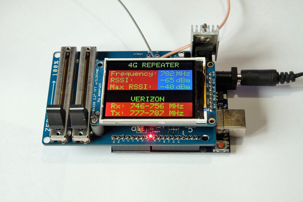
4G Repeater Tuned to Verizon Band 13
09/13/2017 at 09:05 • 1 comment![]() In an attempt to win one of the top 5 Hackaday prizes I've managed to tune a repeater to the Verizon network on band 13 which should, hopefully, work in the USA. I did test the device using the LimeSDR as a signal generator to check that the band filters etc were working properly and ...... all seemed fine.
In an attempt to win one of the top 5 Hackaday prizes I've managed to tune a repeater to the Verizon network on band 13 which should, hopefully, work in the USA. I did test the device using the LimeSDR as a signal generator to check that the band filters etc were working properly and ...... all seemed fine. On this version, there is an AD8218 RSSI chip on the base station Rx pathway which picks up Tx from the mobile phone. Holding my IPhone 7 about 400 mm away from the plate antenna and uploading video to YouTube, I'm getting about -5 dBm max RSSI and holding the phone right next to the antenna gives +10 dBm which is as expected, so it obviously works!
Two more band 13 prototypes need to be built up and all three sent to the USA for appraisal. Better start warming up that soldering iron!
-
Download, Upload and Latency Tests
08/26/2017 at 12:48 • 0 commentsI thought it would be a good idea to do a speed test using my cell phone and compare it's performance whilst using the cell phone repeater in simplex mode and not using it at all.
The result was a decrease in latency from 90 ms to 60 ms and an approximate 6 times increase in download speed!
-
LimeSDR Rigged up for Action
08/22/2017 at 16:45 • 0 commentsThe amazingly flexible and useful LimeSDR is now rigged up with sliders and rotary pots, a TFT screen and bolt on Arduino Due, hiding underneath the green custom made PCB.
The Arduino communicates via the SPI bus through the FPGA using a special file to re-program the FPGA and enables the Lime to be turned from being a 4G repeater into a frequency hopping/sweeping signal generator within literally 5 seconds. I think I can even put 12 LED indicators on it which might look cool?
I need a signal generator to test my homegrown transceivers on band 13 which is what Verizon uses in more remote areas in the USA.
![]()
-
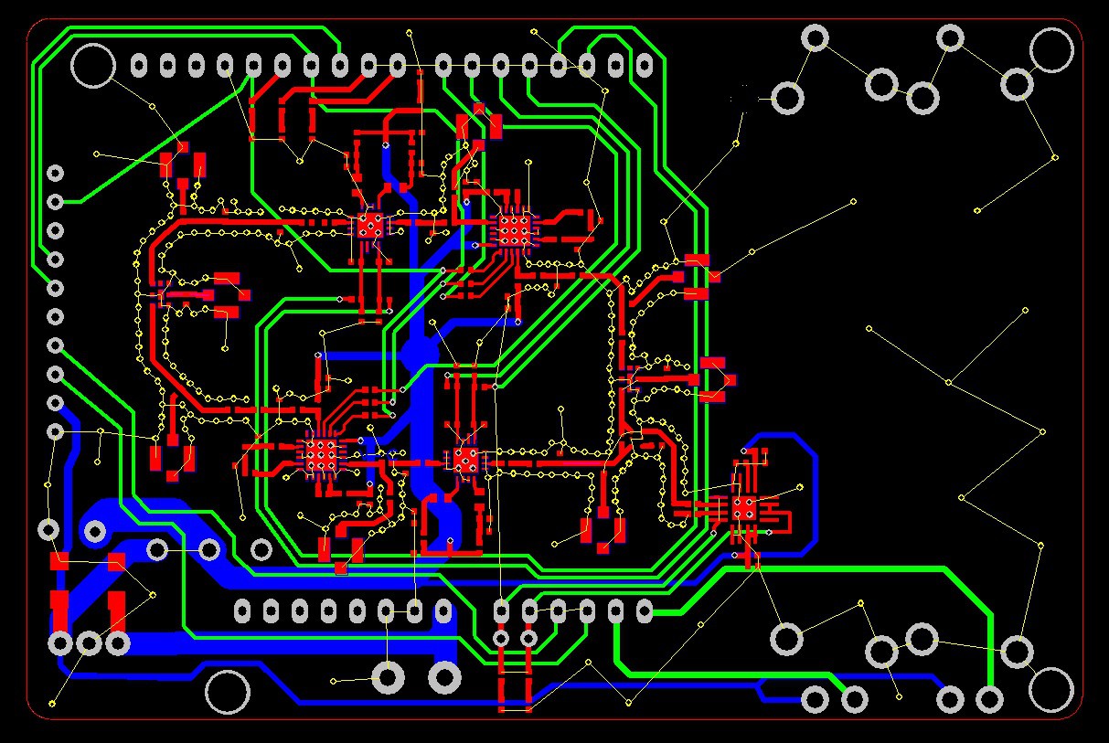
Duplex 09 PCB goes to Manufacturing
08/22/2017 at 16:02 • 0 commentsHopefully this version fixes the voltage supply to the LNA controls by incorporating a simple voltage divider to get exactly 2.5 volts onto the chip. Eventually I should find the one resister to do the job as this will save power, but this is not important at the moment.
I've also added the option to use a RSSI on the phone Tx, just after the band pass filter, which can be used, amongst other things, to confirm that there is a compatible cell phone in the near vicinity. If the phone is detected, it can illuminate one of the spare LEDs to re-assure the user that there is some functionality. The RSSI is connected to the main RF line via a small coupler chip.
I've also got rid of the toggle switch on the power line and replaced it with a more compact slider switch and put it in the correct position, not way off at the top right hand corner. Hopefully this version will be free of any critical errors.
![]()
-
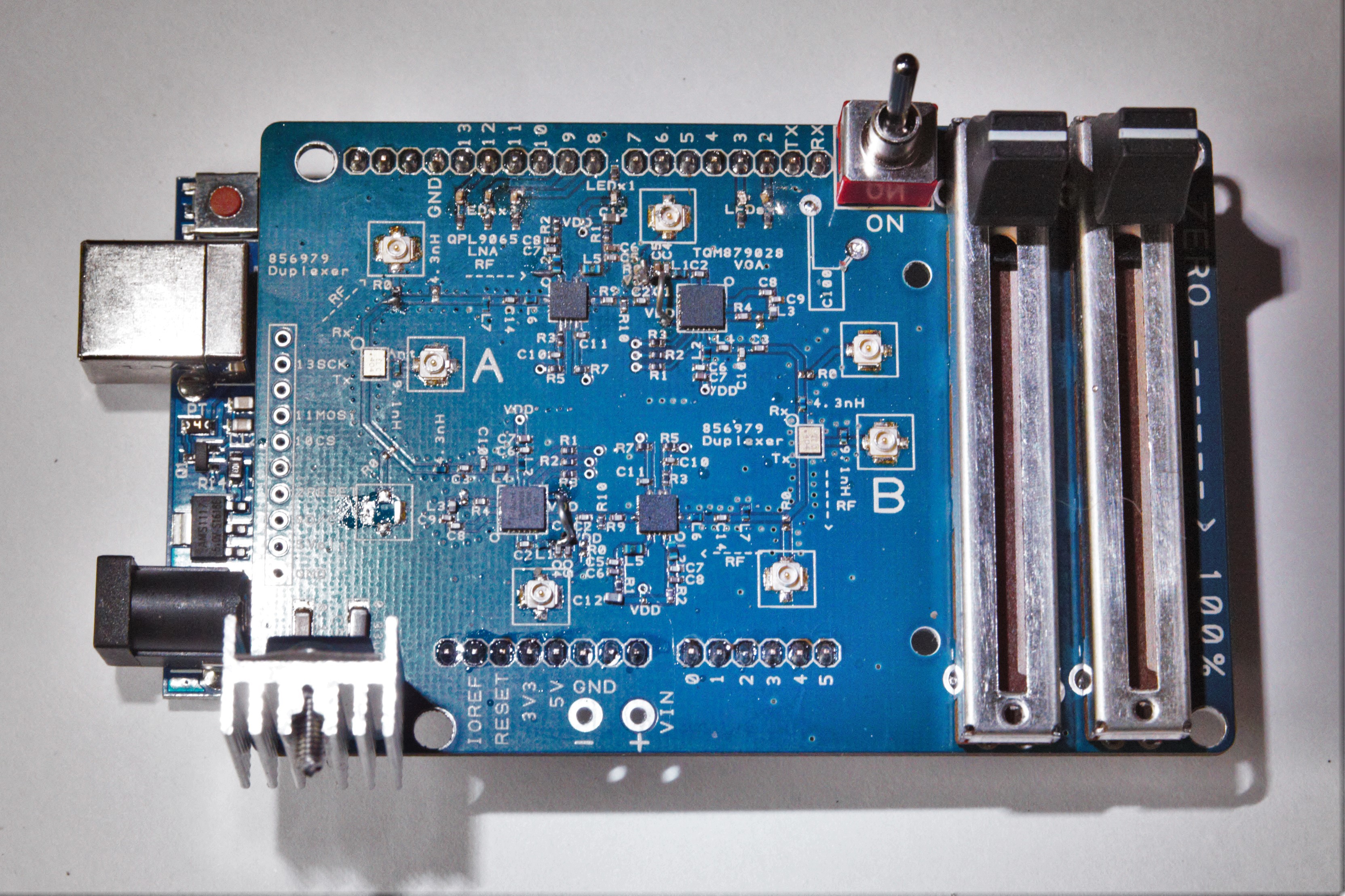
Version 1.1 Duplex board gets populated
08/20/2017 at 14:08 • 1 commentEven with my manual PNP machine, it took a gruelling 6 hours to populate this board below, taking great care to make sure the exact amount of solder was smeared onto the PCB before placing components ..... and still one of the main chips did not work! Thankfully, there are 4 'intercept' points that make the gadget really easy to de-bug and, yes, the VGA worked really nicely on Base Tx frequencies, even though the LNA was bypassed.
![]() It's been a slightly frustrating couple of days, but I did discover 2 fairly serious errors, one of which I corrected with 2 pieces of bare wire. The other mistake was to try and control the LNA's using 5v instead of the recommended 3v - obviously I missed that somehow! Maybe this is why the LNA did not work, rather than bad soldering? Strangely, it did work on the previous incarnation with 5v.
It's been a slightly frustrating couple of days, but I did discover 2 fairly serious errors, one of which I corrected with 2 pieces of bare wire. The other mistake was to try and control the LNA's using 5v instead of the recommended 3v - obviously I missed that somehow! Maybe this is why the LNA did not work, rather than bad soldering? Strangely, it did work on the previous incarnation with 5v.No more work has been done on the LimeSDR this side of the Atlantic although Axeman has picked up my limesuite band 20 .ini file and made certain improvements to it in the USA.
In preparation for creating a Verizon band 13 version, I managed, with the help of Rickardas Jonaitis from Lime Microststems, to create an Arduino controlled signal generator using the LimeSDR. There is no band 13 in the UK and so frequencies have to be generated artificially to test the circuits. The pressure is now on to try and create 3 working prototypes for the Hackaday 2017 finals with the chance to win $50,000. Two months to go!
In the meantime, a short video is being prepared to clarify what the project is about and what the possible solutions are for the BT hackathon final. The actual project challenges seem to be changing fairly rapidly as new information is uncovered or old barriers are pushed through. Currently, the challenge seems to be 'how to safely transmit to the base station without making it crash'. Apparently, gleaned from an expert in the realm of repeaters, noise is a big issue and trying to up convert and down convert should be avoided if at all possible. Maybe simplicity is the answer after all?
Version 1.2 goes to Elecrow PCB service for manufacturing tomorrow.
-
Full Duplex PCB goes to Manufacturer's
08/02/2017 at 17:34 • 0 comments![]() Another 4 layers of abject confusion goes to Shenzhen, hopefully actually correcting a couple of mistakes found in the previous simplex version. Upon re-reading the datasheets for the amps I noticed that through holes are specified for thermal dissipation which should also make it easier to solder the chips, which seemed to me to be floating on a big bubble of solder on the central pad, not allowing the edge pads to make reliable contact. Hopefully that drama is over!
Another 4 layers of abject confusion goes to Shenzhen, hopefully actually correcting a couple of mistakes found in the previous simplex version. Upon re-reading the datasheets for the amps I noticed that through holes are specified for thermal dissipation which should also make it easier to solder the chips, which seemed to me to be floating on a big bubble of solder on the central pad, not allowing the edge pads to make reliable contact. Hopefully that drama is over!Another concern is will there be interference between the two neighbouring circuits? I guess we'll find out in about 10 days time when the boards come back to the UK.
-
Next Big Step: Testing Base Rx Capabilities
07/29/2017 at 18:23 • 0 commentsThe current prototype allows for one of the LNA amps to be bypassed, which seems to be good news for testing the high power part of the circuit where we take the high powered phone signal and transmit it out through the external antenna. With the phone uploading more video to YouTube, the RSSI was recorded on my homemade data capture rig with the antenna about 3 metres in front of the Yagi antenna:
![]() After a few initial spikes, the graph shows a gradual increase in signal strength as the VGA is turned up, reaching something of a plateaux where, presumably, the base station starts telling the phone itself to reduce it's power output.
After a few initial spikes, the graph shows a gradual increase in signal strength as the VGA is turned up, reaching something of a plateaux where, presumably, the base station starts telling the phone itself to reduce it's power output. -
Design Evolution
07/25/2017 at 19:08 • 0 commentsAs time goes on, the plan is evolving and slowly things fall into the right place. The next phase of the project will be to add a Base Rx signal path:
![]()
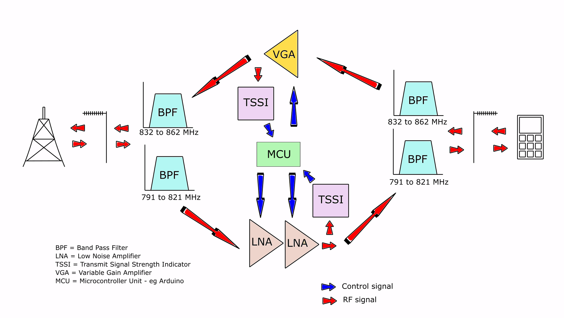
Cell Phone 4G LTE Repeater / Booster / Femtocell
An outside pole mounted aerial picks up 4G signals which are then filtered, amplified and re-transmitted through a second inside aerial.
 In an attempt to win one of the top 5 Hackaday prizes I've managed to tune a repeater to the Verizon network on band 13 which should, hopefully, work in the USA. I did test the device using the LimeSDR as a signal generator to check that the band filters etc were working properly and ...... all seemed fine.
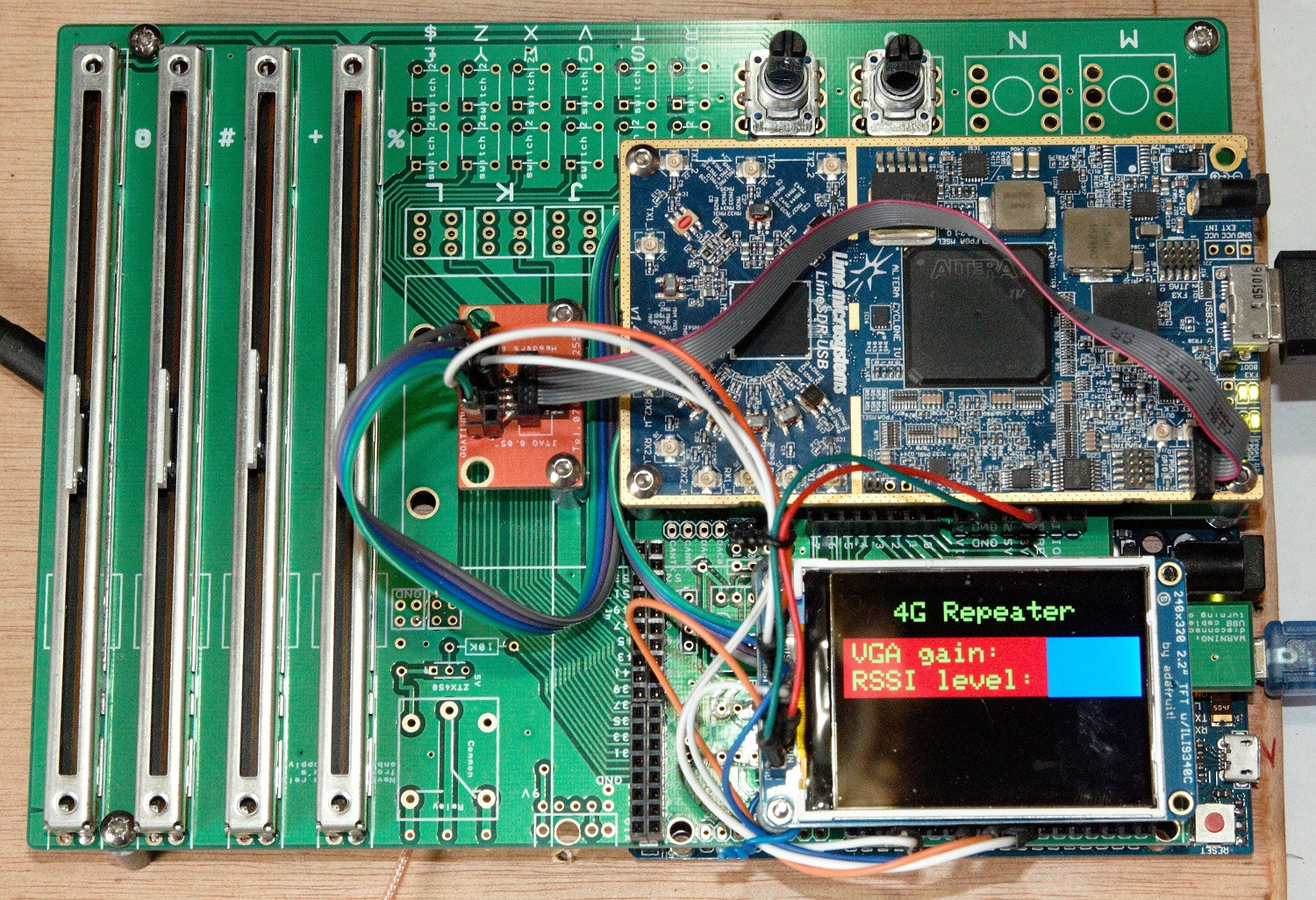
 It's been a slightly frustrating couple of days, but I did discover 2 fairly serious errors, one of which I corrected with 2 pieces of bare wire. The other mistake was to try and control the LNA's using 5v instead of the recommended 3v - obviously I missed that somehow! Maybe this is why the LNA did not work, rather than bad soldering? Strangely, it did work on the previous incarnation with 5v.
 Another 4 layers of abject confusion goes to Shenzhen, hopefully actually correcting a couple of mistakes found in the previous simplex version. Upon re-reading the datasheets for the amps I noticed that through holes are specified for thermal dissipation which should also make it easier to solder the chips, which seemed to me to be floating on a big bubble of solder on the central pad, not allowing the edge pads to make reliable contact. Hopefully that drama is over!
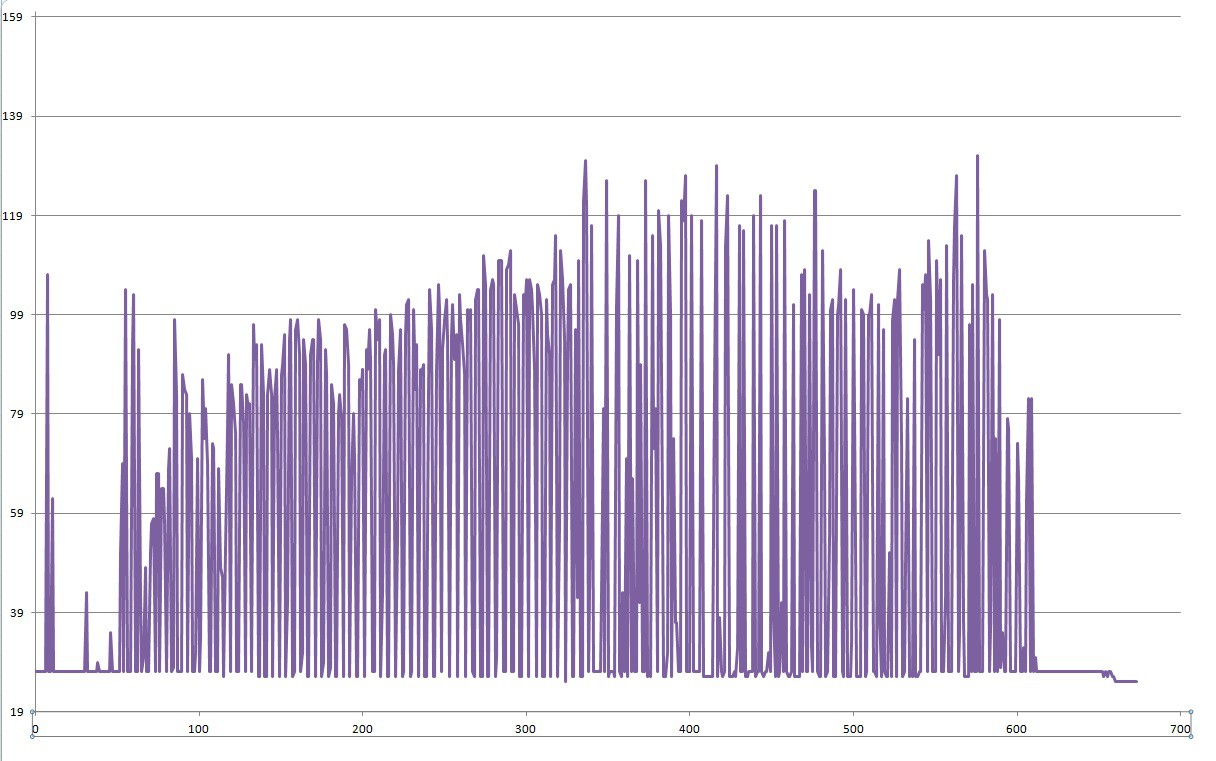 After a few initial spikes, the graph shows a gradual increase in signal strength as the VGA is turned up, reaching something of a plateaux where, presumably, the base station starts telling the phone itself to reduce it's power output.