 Chris
ChrisThe boards are due to be here within the week so now it's finally time to talk about some design decisions. In this case I'm talking about features, compromises, and room for improvement in future revisions, with no particular rhyme or reason.
I/O
First things first is the IO of the Crystal board. At least in my experience, the IO count of an FPGA is a really big deal. For the industries that use them, this makes sense. FPGAs are often used to do real time, true parallel processing by ingesting and fusing input from potentially dozens of sensors while controlling equally as many dozens of output pins. At my day job, we are looking to control about 150 IO in some of our most maximal applications. For context the Arduino Mega lists 54 digital IO. Say what you will, but the best way to get the most IO into an IC is to use a Ball Grid Array package. So considering that FPGAs are often demanded for high pin count applications its no wonder that the vast majority of FPGAs come in ball grid array package.
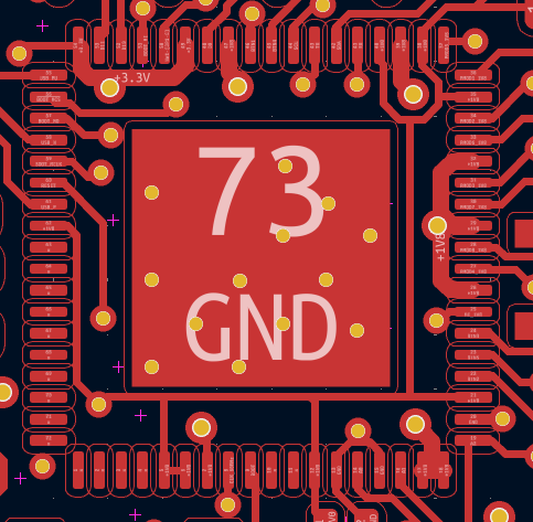
This is starting to get long winded again. Long story short, I wanted an FPGA that was hand-solderable. There are some very nice Gowin FPGAs that are in QFN packages, amongst a few others. I ended up picking the Lattice Crosslink-NX in the QFN package because of its Radiant support. I also think its fun that there is only one ground pin on this bad boy - the center pad.
This was almost a perfect choice for my purposes. The only major bummer is that only about half of the 40 IO on this bad boy is 3.3V compatible, while the read is "high performance" and only supports 1.8V. Most hobbyist electronics still use 3.3V logic and it doesn't seem like that trend is going anywhere soon. Not to say that it couldn't happen (see the switch from 5V logic to 3.3V over the past few years), but regardless, the Adafruit Feather specification requires 3.3V tolerant IO. Plus this is supposed to be user friendly.
Further, I wanted to have buttons, LEDs, and a PMOD connector. This means that I would far exceed the amount of 3.3V logic pins and would need to some level shifting of the 1.8V pins. Even then, I needed to do a lot of doubling up on functions. In retrospect, this isn't that big of a deal. Different MCU boards to that sort of thing all the time, I'm just used to being spoiled by the copious amounts of IO that an FPGA typically provides.
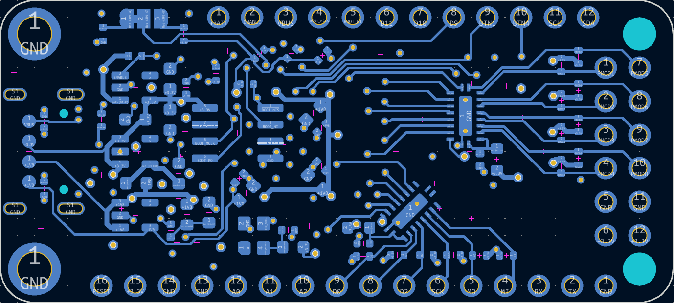 You can see the two level shifters on the right side of the board connecting to pin 4-9, as well as handling the PMOD connector. I am a really big fan of this level shifter. It's bidirectional, high speed, works for up and down translation, and is 8 bits wide. Internally it's basically just a bank of logical level FETs packaged together but that's fine.
This honestly seemed to be a pretty good solution to my lack of 3.3V tolerant IO. I really would like to be able to drive a display using TMDS and an HDMI PMOD, so I am a little concerned that these devices will limit my clock speed too much. Using them in my current configuration, speeds of up to 100MHz signaling are supported but that depends on a lot of factors.
Analog to Digital Converters
We've got them! All of the Nexus platform FPGAs have some pretty decent analog sampling circuitry built into them. There are two parallel ADCs that both can sample at 1 MSPS, which isn't too shabby. On a stock RP2040 the max sample rate is only 500 ksps without overclocking the ADC clock. There are some continuous time comparators as well.
 Based on my IO constraints I was only able to break out 3 pins capable of taking analog samples because for every analog pin it would take up 2 digital IO and I just couldn't spare them. Also, I am using the internal reference, which isn't particularly accurate and limits the measurement voltage to around 1V, sort of an ESP8266 vibe. There is obviously room for improvement here, and sometime I want to take another look at in future revisions of the board.
Buttons and LEDs
Considering my target audience and applications, plenty of buttons and LEDs are needed for this board. In total there are 4 LEDs and 6 buttons. A very popular project for into FPGA classes is the binary counter, so I wanted to make sure that there was more than just the typical pin number 13 LED. I couldn't figure out a great way to fit more than 4 lights on there so I figured that was good enough.
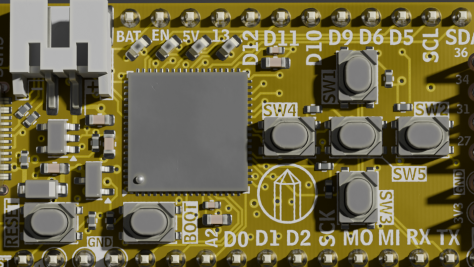
The number and arrangement of buttons might be interesting to some folks, but let me explain. At least in the FPGA class that I taught, one of the most popular final projects is to make a video game. There have been some amazing implementations of Frogger, Snake, Simon, even Spy Hunter.
However, on the Zybo Z7 board, the four buttons are arranged in a horizontal line. Despite having used Vim (come at me) for a number of years, my brain breaks when I play a students game on those horizontal buttons. So you'll notice that I arranged them in the shape of a game pad, Gameboy style. If there is an HDMI PMOD hanging of the side with a cable coming out of it, you can almost hold it like a controller! It's the little things...
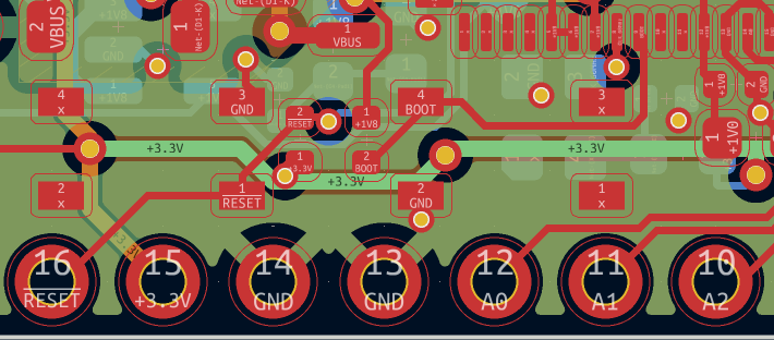
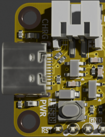
Lipo Charger
We want to be fully feather compatible so that means a Lipo charger. Initially I was a bit reluctant to comply with this aspect of the Feather formfactor. After some reflection, there are a decent amount of final projects in my class that wanted to drive higher current devices like motors, so adding a battery into the mix is actually an easy way to source more than the approx. 10 mA per pin that this FPGA can do. Just a single LED to indicate charge state, with the battery diode OR'ed into the regulators. Current is fixed at 100 mA or something.
USB
This is probably one of the riskier parts of design. The physical connector is just a USB-C with the proper CC1 and CC2 resistors. However, in order to save some money and board space, I am skipping the typical FTDI usb converter. Alternatively, it would be relatively easy to use an MCU to act like a converter chip, while also adding features to the board. Both the Pico-Ice and the Tang Nano 20k come to mind for this approach. But honestly I didn't want monkey around with all that added complexity.
Instead, I am taking advantage of the fact that FPGAs are magic and can do almost anything. I am hooking up the USB D+ and D- pins directly to the FPGA pins along with a pull up resistor on a third pin that is use for enumeration. That is technically all the circuitry you need. The rest is handled inside the FPGA. I need to double check all the licensing and what not, but my plan is to use the resources provided by this absolutely amazing repository.
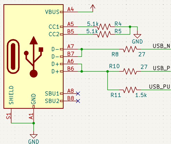
Gigantic shout out to [WangXuan95] for publishing that HDL. With just three IO, we can now have a nominal 12 mbps serial device with no added chips or cost. The added bonus here is that because we are never actually converting to a typical RX and TX line of a UART, we never need to worry about incorrectly set baud rates! I'm excited to explore the USB mass storage storage USB endpoint implementation as well to hopefully enable a drag and drop programming paradigm.
Discussions
Become a Hackaday.io Member
Create an account to leave a comment. Already have an account? Log In.