Affordable AND useful digital logic design. Finally.
To make the experience fit your profile, pick a username and tell us what interests you.
We found and based on your interests.
fpga_board.pdfAdobe Portable Document Format - 584.72 kB - 03/21/2026 at 23:35 |
|
|
Okay finally, finally, finally we have caught up to real time. We have hardware (YESSSSS).
For the 1-2 of the people who'd actually like to see this project come to light, this is a big deal.
First and foremost, I'd like to thank PCBWay for sponsoring this project. Say what you will, but if it wasn't for [Aran] from PCBWay reaching out and asking if I had any projects going on, this whole thing probably would have never gotten off the ground. I'd also like to note that everything in this post is my truthful opinion.
If you are looking for some high qualify PCB manufacturing services, you really can't beat them. Of course, there are plenty of places to get PCBs made these days, but honestly what impressed the hell out of me was the assembly service.
I have explored other vendors for assembly services before and wasn't super impressed, finding the process more difficult than just putting together the boards myself. PCBWay was a completely different story.
They were super attentive through the whole process, and even suggested alternate parts when some of my BoM items weren't available. They were also able to pick suitable jellybean components with minimal input from me. All of the procurement and shipping of my requested parts was handled without a single issue. PCBWay even sends an image of the assembled PCB before shipping to ensure that all components have been placed in their correct orientation and that no further rework is needed - incredible. The boards got a tracking number and showed up about a week later.
If you've ever been hesitant to explore assembly options from PCBWay, you may want to reconsider. The entire process was smooth, affordable, and professional. Seriously, the whole process was incredible.
Continuing, the rest of this post will be mostly eye-candy and visual inspection of the PCBs. I will then finish the post with next steps.
Starting generally, the PCBs look awesome. These are the first yellow PCBs that I have ever ordered and PCBWay did not disappoint with the color. I choose to go with a yellow soldermask because of the Lattice CrossLink-NX chip that I am using. Go team yellow!
I received the boards almost entirely populated. I chose to omit the FPGA from the assembly BoM. This was just for cost and logistic reasons related to the sponsorship.
Before shipping and fees, the cost of 5 assembled boards + components (minus FPGA) was $99.55. According to the invoice, the unit price was $19.67 per board in quantity x5. However, keep in mind that the LIFCL-17-8SG72C is currently priced on Digikey at $19.75, with that dropping to around $15 at a qty. of 100.
So the BoM cost comes in around $40 dollars in single quantities. This mostly aligns with our $50 dollar price point, and I think there is some further room for cost optimization.
With the boring stuff out of the way here are some nice pretty pictures from my microscope, starting off with just a shot of the FPGA. I used hotair to stick on the QFN-72 package, and then ran the tip of my iron around the edge of the board to make sure that my joints looked alright. I didn't do a very good job cleaning the gunk off afterwards. You'll also noticed the little bit of melty-melt on the JST connector and SW4 -that's my bad. It's been a while since I have soldered something in such close quarters. Embarrassing!
Next up I took a look at the silkscreen. In my effort for self documenting PCBs, I tend to push the limits in this area. However, this time around it looks pretty good! I believe that the go-to option for printing text on PCBs is now some sort of inkjet process (as opposed to true silkscreen).
This is a topic that I have explored in the past, but frankly the resolution here is acceptable, and everything seems pretty consistent.
The boards are due to be here within the week so now it's finally time to talk about some design decisions. In this case I'm talking about features, compromises, and room for improvement in future revisions, with no particular rhyme or reason.
First things first is the IO of the Crystal board. At least in my experience, the IO count of an FPGA is a really big deal. For the industries that use them, this makes sense. FPGAs are often used to do real time, true parallel processing by ingesting and fusing input from potentially dozens of sensors while controlling equally as many dozens of output pins. At my day job, we are looking to control about 150 IO in some of our most maximal applications. For context the Arduino Mega lists 54 digital IO. Say what you will, but the best way to get the most IO into an IC is to use a Ball Grid Array package. So considering that FPGAs are often demanded for high pin count applications its no wonder that the vast majority of FPGAs come in ball grid array package.
This is starting to get long winded again. Long story short, I wanted an FPGA that was hand-solderable. There are some very nice Gowin FPGAs that are in QFN packages, amongst a few others. I ended up picking the Lattice Crosslink-NX in the QFN package because of its Radiant support. I also think its fun that there is only one ground pin on this bad boy - the center pad.
This was almost a perfect choice for my purposes. The only major bummer is that only about half of the 40 IO on this bad boy is 3.3V compatible, while the read is "high performance" and only supports 1.8V. Most hobbyist electronics still use 3.3V logic and it doesn't seem like that trend is going anywhere soon. Not to say that it couldn't happen (see the switch from 5V logic to 3.3V over the past few years), but regardless, the Adafruit Feather specification requires 3.3V tolerant IO. Plus this is supposed to be user friendly.
Further, I wanted to have buttons, LEDs, and a PMOD connector. This means that I would far exceed the amount of 3.3V logic pins and would need to some level shifting of the 1.8V pins. Even then, I needed to do a lot of doubling up on functions. In retrospect, this isn't that big of a deal. Different MCU boards to that sort of thing all the time, I'm just used to being spoiled by the copious amounts of IO that an FPGA typically provides.
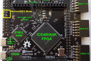
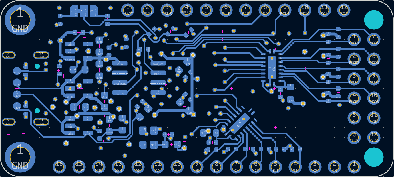
You can see the two level shifters on the right side of the board connecting to pin 4-9, as well as handling the PMOD connector. I am a really big fan of this level shifter. It's bidirectional, high speed, works for up and down translation, and is 8 bits wide. Internally it's basically just a bank of logical level FETs packaged together but that's fine.
This honestly seemed to be a pretty good solution to my lack of 3.3V tolerant IO. I really would like to be able to drive a display using TMDS and an HDMI PMOD, so I am a little concerned that these devices will limit my clock speed too much. Using them in my current configuration, speeds of up to 100MHz signaling are supported but that depends on a lot of factors.
We've got them! All of the Nexus platform FPGAs have some pretty decent analog sampling circuitry built into them. There are two parallel ADCs that both can sample at 1 MSPS, which isn't too shabby. On a stock RP2040 the max sample rate is only 500 ksps without overclocking the ADC clock. There are some continuous time comparators as well.
Let me first admit at the time of writing this the boards have already been ordered, simply for the fact that I didn't want to lose my momentum on this project. All too often I have let perfection be the enemy of good and I am determined to try to break the cycle. For the same reason I intend to write this first project log in a stream-of-consciousness style that may feel rather messy. Nevertheless, writing something is better than nothing. Hopefully it's coherent and I get my points across.
In this log I mainly want to talk about the motivation for this project, and talk about the current state of the FPGA hobbyist world from my perspective.
As I mentioned in the description, this project is meaningful to me on a personal level. Over the past few years I have had the opportunity to interact very closely with my local university and their FPGA design class. I work very closely with the professor at my day job as an FPGA engineer, so every year I get to chat with students, grade final projects, interview prospective interns. Just this past semester, I even got to teach part of the course as an adjunct professor.
I really like FPGAs. I think about them almost constantly. I think they are just about the coolest electronic invention ever and its a joy that I get to work with them everyday. Not only that, I absolutely love teaching other people about FPGAs too. Just imagine: a magical IC that can basically take the form of any digital circuit, even a CPU! Of course, not everyone is interested, or even sees/understands the potential in the devices, which is fine. However, every semester there are a handful of students that "get it." It clicks for them just how powerful these devices can be and they understand why I get so excited about the subject. The problem is that after the class ends, these students are mostly abandoned.
Currently, in class use the Zybo Z7 board, and with one board rented out to a pair of lab partners. After the final project has been completed, the lab partners must then turn in their boards and get on with their well earned winter break. So this model not only encourages an unfair distribution of labor ("I will write the VHDL and you can do the report" often turns into, "I just did the whole lab by myself"), it also completely disqualifies the genuinely curious student from any tinkering or experimentation after the semester has ended. Not to mention using an FPGA in their upcoming senior design projects. It's really a bummer because every semester there is at least a handful of students who:
Over the past few years of interacting with these students and the university here are the answer to the inquires above
It's this last point I want to focus on.
You might be telling yourself "surely there are plenty of good options out there." You have probably even seen some decent attempts, and honestly, fair play. There have been plenty of decent attempts, but not for not for someone using who wants to use an FPGA on their own workbench or in their dorm room. Let's me highlight a few of my favorites, and address their short comings.
Probably one of the most popular entry level FPGA dev boards and targeted specifically for students and workshops. Based on the ICE40 FPGA from Lattice, it's a strong contender, especially with the open source tool chain. At 80 dollars though, that might be worth a week or two of groceries for the frugal college student. Moreover, the form factor is bizarre...
Read more »
Create an account to leave a comment. Already have an account? Log In.
Become a member to follow this project and never miss any updates
Jarrett
Jared
John Adams
Have you looked at circuitverse?
It seems to me that this provides almost no barrier to entry to anyone wanting to play with FPGAs for the first time. So is perhaps a good solution as an entry point for users in the wider feather ecosystem.
Perhaps it provides a pathway to introduce proper tools.