Chris
Chris-
Hardware is Here (+ PCBWay Shoutout)
an hour ago • 0 commentsOkay finally, finally, finally we have caught up to real time. We have hardware (YESSSSS).
For the 1-2 of the people who'd actually like to see this project come to light, this is a big deal.
Sponsorship
First and foremost, I'd like to thank PCBWay for sponsoring this project. Say what you will, but if it wasn't for [Aran] from PCBWay reaching out and asking if I had any projects going on, this whole thing probably would have never gotten off the ground. I'd also like to note that everything in this post is my truthful opinion.
![]()
If you are looking for some high qualify PCB manufacturing services, you really can't beat them. Of course, there are plenty of places to get PCBs made these days, but honestly what impressed the hell out of me was the assembly service.I have explored other vendors for assembly services before and wasn't super impressed, finding the process more difficult than just putting together the boards myself. PCBWay was a completely different story.
They were super attentive through the whole process, and even suggested alternate parts when some of my BoM items weren't available. They were also able to pick suitable jellybean components with minimal input from me. All of the procurement and shipping of my requested parts was handled without a single issue. PCBWay even sends an image of the assembled PCB before shipping to ensure that all components have been placed in their correct orientation and that no further rework is needed - incredible. The boards got a tracking number and showed up about a week later.
If you've ever been hesitant to explore assembly options from PCBWay, you may want to reconsider. The entire process was smooth, affordable, and professional. Seriously, the whole process was incredible.
Continuing, the rest of this post will be mostly eye-candy and visual inspection of the PCBs. I will then finish the post with next steps.
The Hardware
Starting generally, the PCBs look awesome. These are the first yellow PCBs that I have ever ordered and PCBWay did not disappoint with the color. I choose to go with a yellow soldermask because of the Lattice CrossLink-NX chip that I am using. Go team yellow!
I received the boards almost entirely populated. I chose to omit the FPGA from the assembly BoM. This was just for cost and logistic reasons related to the sponsorship.

Unpopulated Crystal Board Before shipping and fees, the cost of 5 assembled boards + components (minus FPGA) was $99.55. According to the invoice, the unit price was $19.67 per board in quantity x5. However, keep in mind that the LIFCL-17-8SG72C is currently priced on Digikey at $19.75, with that dropping to around $15 at a qty. of 100.
So the BoM cost comes in around $40 dollars in single quantities. This mostly aligns with our $50 dollar price point, and I think there is some further room for cost optimization.
With the boring stuff out of the way here are some nice pretty pictures from my microscope, starting off with just a shot of the FPGA. I used hotair to stick on the QFN-72 package, and then ran the tip of my iron around the edge of the board to make sure that my joints looked alright. I didn't do a very good job cleaning the gunk off afterwards. You'll also noticed the little bit of melty-melt on the JST connector and SW4 -that's my bad. It's been a while since I have soldered something in such close quarters. Embarrassing!

Money Shot of the FPGA Next up I took a look at the silkscreen. In my effort for self documenting PCBs, I tend to push the limits in this area. However, this time around it looks pretty good! I believe that the go-to option for printing text on PCBs is now some sort of inkjet process (as opposed to true silkscreen).
This is a topic that I have explored in the past, but frankly the resolution here is acceptable, and everything seems pretty consistent.

Large silkscreen features look good 
What a cool logo! The smallest text I have on this board is for the voltage regulator test points located under the USB-C connector. These measure a mere 0.5x0.5mm according to KiCAD. The physical results are hardly impressive, but the text is identifiable! There was also a little bit of an issue with particularly fine lines around through, holes but again, this is me mostly just pushing the process a bit too far.

Itty Bitty Testpoint Label 
Fine lines are hard!
Moving away from cosmetics, I also took a look at solder joint quality and via registration. Both of which seemed to be acceptable considering the cost of these boards.There were a few examples of solder joints that didn't appear to be fully wetted, or maybe a little too much solder paste.
When it comes to the LEDs, I think that may just be how they are intended to be reflowed (as opposed to having the solder flow up and on top of the contacts).
LEDs Chillin 
Another Part of the Board 
Via shot and too much solder On the LSF0108 chip above, you can see the pretty clear beading of the solder on the joints. If I were to guess, this is mostly my fault, and I probably didn't pay attention to what the solder past distribution was supposed to look like when I was making the footprint in KiCAD. None of the pins are shorting, which is the important part.
You can also see from the images above the the vias are mostly in the center of their pads. Mostly. Importantly, none of the vias broke out of their annular rings, at least that I can tell.
Next Steps
So now that we have the boards, what's next? So far I have plugged in the board to a USB-C port and no smoke came out. Good! All of the voltage rails measured well which means that nothing is shorting out (either because of a manufacturing defect or routing issue).
That means the next order of business is to get this thing hooked up to a traditional JTAG programmer and see if I can get an LED blinking! From there I will move on to implementing a bootloader.
-
Design Choices
03/21/2026 at 23:32 • 0 commentsThe boards are due to be here within the week so now it's finally time to talk about some design decisions. In this case I'm talking about features, compromises, and room for improvement in future revisions, with no particular rhyme or reason.
I/O
First things first is the IO of the Crystal board. At least in my experience, the IO count of an FPGA is a really big deal. For the industries that use them, this makes sense. FPGAs are often used to do real time, true parallel processing by ingesting and fusing input from potentially dozens of sensors while controlling equally as many dozens of output pins. At my day job, we are looking to control about 150 IO in some of our most maximal applications. For context the Arduino Mega lists 54 digital IO. Say what you will, but the best way to get the most IO into an IC is to use a Ball Grid Array package. So considering that FPGAs are often demanded for high pin count applications its no wonder that the vast majority of FPGAs come in ball grid array package.
This is starting to get long winded again. Long story short, I wanted an FPGA that was hand-solderable. There are some very nice Gowin FPGAs that are in QFN packages, amongst a few others. I ended up picking the Lattice Crosslink-NX in the QFN package because of its Radiant support. I also think its fun that there is only one ground pin on this bad boy - the center pad.![]()
This was almost a perfect choice for my purposes. The only major bummer is that only about half of the 40 IO on this bad boy is 3.3V compatible, while the read is "high performance" and only supports 1.8V. Most hobbyist electronics still use 3.3V logic and it doesn't seem like that trend is going anywhere soon. Not to say that it couldn't happen (see the switch from 5V logic to 3.3V over the past few years), but regardless, the Adafruit Feather specification requires 3.3V tolerant IO. Plus this is supposed to be user friendly.
Further, I wanted to have buttons, LEDs, and a PMOD connector. This means that I would far exceed the amount of 3.3V logic pins and would need to some level shifting of the 1.8V pins. Even then, I needed to do a lot of doubling up on functions. In retrospect, this isn't that big of a deal. Different MCU boards to that sort of thing all the time, I'm just used to being spoiled by the copious amounts of IO that an FPGA typically provides.
![]() You can see the two level shifters on the right side of the board connecting to pin 4-9, as well as handling the PMOD connector. I am a really big fan of this level shifter. It's bidirectional, high speed, works for up and down translation, and is 8 bits wide. Internally it's basically just a bank of logical level FETs packaged together but that's fine.
You can see the two level shifters on the right side of the board connecting to pin 4-9, as well as handling the PMOD connector. I am a really big fan of this level shifter. It's bidirectional, high speed, works for up and down translation, and is 8 bits wide. Internally it's basically just a bank of logical level FETs packaged together but that's fine. ![]()
This honestly seemed to be a pretty good solution to my lack of 3.3V tolerant IO. I really would like to be able to drive a display using TMDS and an HDMI PMOD, so I am a little concerned that these devices will limit my clock speed too much. Using them in my current configuration, speeds of up to 100MHz signaling are supported but that depends on a lot of factors.
Analog to Digital Converters
We've got them! All of the Nexus platform FPGAs have some pretty decent analog sampling circuitry built into them. There are two parallel ADCs that both can sample at 1 MSPS, which isn't too shabby. On a stock RP2040 the max sample rate is only 500 ksps without overclocking the ADC clock. There are some continuous time comparators as well.
![]() Based on my IO constraints I was only able to break out 3 pins capable of taking analog samples because for every analog pin it would take up 2 digital IO and I just couldn't spare them. Also, I am using the internal reference, which isn't particularly accurate and limits the measurement voltage to around 1V, sort of an ESP8266 vibe. There is obviously room for improvement here, and sometime I want to take another look at in future revisions of the board.
Based on my IO constraints I was only able to break out 3 pins capable of taking analog samples because for every analog pin it would take up 2 digital IO and I just couldn't spare them. Also, I am using the internal reference, which isn't particularly accurate and limits the measurement voltage to around 1V, sort of an ESP8266 vibe. There is obviously room for improvement here, and sometime I want to take another look at in future revisions of the board.
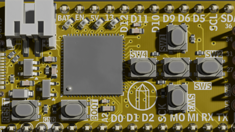
Buttons and LEDs
Considering my target audience and applications, plenty of buttons and LEDs are needed for this board. In total there are 4 LEDs and 6 buttons. A very popular project for into FPGA classes is the binary counter, so I wanted to make sure that there was more than just the typical pin number 13 LED. I couldn't figure out a great way to fit more than 4 lights on there so I figured that was good enough.
![]()
The number and arrangement of buttons might be interesting to some folks, but let me explain. At least in the FPGA class that I taught, one of the most popular final projects is to make a video game. There have been some amazing implementations of Frogger, Snake, Simon, even Spy Hunter.
However, on the Zybo Z7 board, the four buttons are arranged in a horizontal line. Despite having used Vim (come at me) for a number of years, my brain breaks when I play a students game on those horizontal buttons. So you'll notice that I arranged them in the shape of a game pad, Gameboy style. If there is an HDMI PMOD hanging of the side with a cable coming out of it, you can almost hold it like a controller! It's the little things...
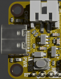
Lipo Charger
We want to be fully feather compatible so that means a Lipo charger. Initially I was a bit reluctant to comply with this aspect of the Feather formfactor. After some reflection, there are a decent amount of final projects in my class that wanted to drive higher current devices like motors, so adding a battery into the mix is actually an easy way to source more than the approx. 10 mA per pin that this FPGA can do. Just a single LED to indicate charge state, with the battery diode OR'ed into the regulators. Current is fixed at 100 mA or something.
![]()
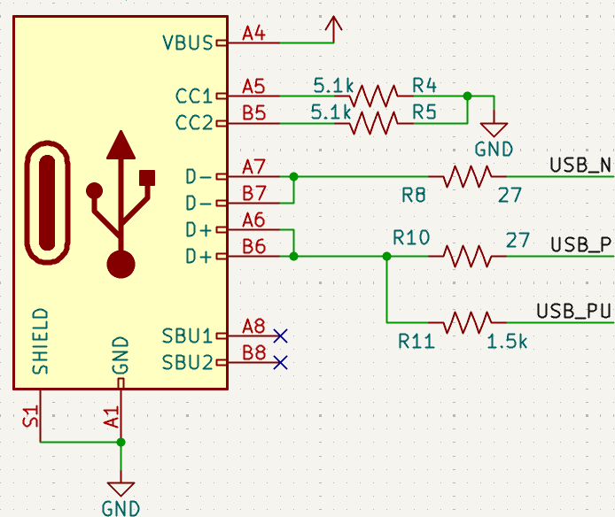
USB
This is probably one of the riskier parts of design. The physical connector is just a USB-C with the proper CC1 and CC2 resistors. However, in order to save some money and board space, I am skipping the typical FTDI usb converter. Alternatively, it would be relatively easy to use an MCU to act like a converter chip, while also adding features to the board. Both the Pico-Ice and the Tang Nano 20k come to mind for this approach. But honestly I didn't want monkey around with all that added complexity.
Instead, I am taking advantage of the fact that FPGAs are magic and can do almost anything. I am hooking up the USB D+ and D- pins directly to the FPGA pins along with a pull up resistor on a third pin that is use for enumeration. That is technically all the circuitry you need. The rest is handled inside the FPGA. I need to double check all the licensing and what not, but my plan is to use the resources provided by this absolutely amazing repository.
![]()
Gigantic shout out to [WangXuan95] for publishing that HDL. With just three IO, we can now have a nominal 12 mbps serial device with no added chips or cost. The added bonus here is that because we are never actually converting to a typical RX and TX line of a UART, we never need to worry about incorrectly set baud rates! I'm excited to explore the USB mass storage storage USB endpoint implementation as well to hopefully enable a drag and drop programming paradigm.
Conclusion
That wraps up most of the good stuff. I tried to cover what I thought was interesting and important without being too long winded. Obviously I'd love to answer any specific questions that people might have in the comments. We now have TWO whole comments and I feel like I'm on top of the world. Hopefully the next log will show some actual hardware -
Motivation & Decent Alternatives
03/16/2026 at 00:49 • 0 commentsLet me first admit at the time of writing this the boards have already been ordered, simply for the fact that I didn't want to lose my momentum on this project. All too often I have let perfection be the enemy of good and I am determined to try to break the cycle. For the same reason I intend to write this first project log in a stream-of-consciousness style that may feel rather messy. Nevertheless, writing something is better than nothing. Hopefully it's coherent and I get my points across.
In this log I mainly want to talk about the motivation for this project, and talk about the current state of the FPGA hobbyist world from my perspective.
Motivation
Preface
As I mentioned in the description, this project is meaningful to me on a personal level. Over the past few years I have had the opportunity to interact very closely with my local university and their FPGA design class. I work very closely with the professor at my day job as an FPGA engineer, so every year I get to chat with students, grade final projects, interview prospective interns. Just this past semester, I even got to teach part of the course as an adjunct professor.
I really like FPGAs. I think about them almost constantly. I think they are just about the coolest electronic invention ever and its a joy that I get to work with them everyday. Not only that, I absolutely love teaching other people about FPGAs too. Just imagine: a magical IC that can basically take the form of any digital circuit, even a CPU! Of course, not everyone is interested, or even sees/understands the potential in the devices, which is fine. However, every semester there are a handful of students that "get it." It clicks for them just how powerful these devices can be and they understand why I get so excited about the subject. The problem is that after the class ends, these students are mostly abandoned.
Currently, in class use the Zybo Z7 board, and with one board rented out to a pair of lab partners. After the final project has been completed, the lab partners must then turn in their boards and get on with their well earned winter break. So this model not only encourages an unfair distribution of labor ("I will write the VHDL and you can do the report" often turns into, "I just did the whole lab by myself"), it also completely disqualifies the genuinely curious student from any tinkering or experimentation after the semester has ended. Not to mention using an FPGA in their upcoming senior design projects. It's really a bummer because every semester there is at least a handful of students who:- inquire about keeping their boards for longer,
- want to buy the FPGA dev board for themselves
- ask for decent alternative FPGA boards
Over the past few years of interacting with these students and the university here are the answer to the inquires above
- The department gives some strong discouragement for doing so. (Must be enrolled, doing research, they are expensive etc.)
- They are about 299 dollars at the time of writing. That's just not happening for a college student.
- There are no decent alternatives. Not really.
It's this last point I want to focus on.
No Decent Alternatives
You might be telling yourself "surely there are plenty of good options out there." You have probably even seen some decent attempts, and honestly, fair play. There have been plenty of decent attempts, but not for not for someone using who wants to use an FPGA on their own workbench or in their dorm room. Let's me highlight a few of my favorites, and address their short comings.
ICEBreaker
Probably one of the most popular entry level FPGA dev boards and targeted specifically for students and workshops. Based on the ICE40 FPGA from Lattice, it's a strong contender, especially with the open source tool chain. At 80 dollars though, that might be worth a week or two of groceries for the frugal college student. Moreover, the form factor is bizarre at best. Points for the 0.1" header but good luck putting that on a breadboard. I'm also happy to see the bountiful PMOD ports but, unless you are already "into" FPGAs, I doubt that most students or hackers have even know what that is, much less have a collection of PMOD compatible boards laying around. Comparing a PMOD to the availability of an Arduino shield, Adafruit Feather Wing, or Raspberry Pi Hat, there is no contest. I have some more thoughts on the tool chain situation, but will save that for its own section
Arty A7 Board
Another very common FPGA board that I see in various enthusiasts posts. First of all, the price. We are talking 300 dollars here. No. Just no. that's a crazy amount of money for an entry level FPGA board unless you are a University performing a bulk buy or a major corporation that has no problem paying for equipment with more zeros on the price tag than what the average hacker is used to seeing. Frankly, with the price, the rest of the capabilities almost aren't worth talking about.
I will award a few minor bonus points though. 1) being that there is an Arduino shield compatible header. So obviously some amount of thought went into what people might want to use this board for. An appeal to the common person. 2) Vivado is definitely one of the most cohesive HDL IDEs out there that doesn't make me want to immediately open vim and write a TCL script (more thoughts on Vivado at the end).
Also worth mentioning is the Arty S7 board which comes in at a slightly less eye watering price. Both the A7 and the S7 make the claim that the they were designed with "versatility and flexibility" in mind. Which is great! But the fact is that they obviously "kept it in mind" rather than "prioritized" it. Neither the S7 or the A7 even have mounting holes!
Tiny FPGA Series
Ah the TinyFPGA! One of the shining starts of the hobbyist FPGA world, but taken from us too soon. Honestly, this line of boards checks nearly all the boxes. In my mind they are the FPGA parallel to the Teensy series of MCU boards, which may have even been the intention. Of course they are based on the ICE40 from Lattice so you have the freely available tool chain. They are breadboard compatible, the first of the devices covered here, and they were reasonably priced. My favorite feature on this series of boards however, is the bootloader.
Actually programming an FPGA board is another aspect of this world that is often glossed over with FTDI converter chips (which add cost and size) and propriety and/or recommended external programmers. Many of these programmers often cost over $100 alone! Luke Valenty got it right - it's an FPGA you can make it do pretty much whatever you want. Why not whip up a "DFU" mode just like every microcontroller out there?
But Alas, it appears the TinyFPGA is mostly abandoned. I will admit that I am not entirely up to date on the subject, but I believe an ECP5 version of the series was planned which would have given a major upgrade to the LUT count of these devices. The roughly 5-8k LUT limitation with negligible math blocks is really my only complaint about the boards that were available for a time.
Tang Nano 20k
Oh we are so close with the Tang Nano 20k. We have nearly all the marks. They have an INCREDIBLE price point at under $50 and you can get them on Amazon. They are breadboard compatible. They have a super duper reasonable amount of LUTs, BRAM, and math blocks - 20k LUTS starts making it feel "real" FPGA and not just an entry level toy. And finally, an open source tool chain that is being actively maintained and improved (thank you so much @yrabbit.)
So then what's the problem? I'm not entirely sure. I think the reason that you don't see these boards in every single lab space and lecture hall is mostly an issue of marketing and not being "mainstream." The Tang Nano 20k is primarily marketed around retrogaming, which admittedly makes up a relatively large portion of the hobbyist FPGA community. It has a small connector for audio out, a flex connector for a TFT screen, and an HDMI port (!). All to help you recreate and the consoles of yesteryears. The board was designed for a specific purpose for SiSpeed, and honestly, that's okay. In regards to the other "mainstream" comment: these boards are based on Gowin FPGAs. This is a Chinese FPGA company that make some really impressive devices at an incredible price point, and with decent documentation. At the end of the day I think it's just hard for a Chinese company to get traction in an industry dominated by some pretty gigantic American corporations. I believe the their IDE leaves something to be desired as well.
I have many more thoughts and questions on Gowin as whole but I will save that for another time.
CMOD
Last but not least is the CMOD board. Again, here we have a very reasonable contender for my goal of a well rounded general purpose FPGA board for the student and hacker. It's breadboard compatible, and comes with a single PMOD port. You don't need an external programmer and with 32 IO and even a couple analog inputs it's pretty compelling. The issue? The price! 100 dollars is definitely not as bad as it could be, but I personally still would think twice about dropping that kind of money, especially given the very real possibility I could blow it up. Further more, there is the whole "Vivado" thing, which applies to the Arty boards discussed above, as well. See the following section.
IDE / Tool Chain
This post is already long and rambling, and frankly I'm getting tired of writing, but I am going to do another long winded dive into on the subject of IDEs and toolchains. In short, they matter.
In Defense of Simple
In my opinion, a major key to the success the original Arduino Uno's was the IDE. It was simple, easy, and ready to go. There was no need to understand compilers, linkers, or assemblers. You just hit the compile and then upload button and boom - you are blinking and LED. Many said that this wasn't "real" embedded programming, and to them I say "shame on you!" The Arduino IDE is/was limited and basic enough that it gets out of your way. There is no need to deal with a multiplicative set of learning curves of both digital electronics and toolchain setup at the same time, especially when one was just interested learning more about electronics or trying to add lights to their Halloween costume or something. It handled all that setup for you. A further example can be seen in the traditional Arduino serial terminal. The user didn't really need to know anything about UARTs or USB converter chips or baud rates or ASCII if they didn't want to. At the end of the day, copying and pasting a snippet of code that let you print values to the screen was good enough.
No one has really provided a ubiquitous "Arduino IDE" for FPGAs as a whole. A piece of software that says "No no, I will take care of all the messy stuff behind the scenes - just focus on writing your HDL." This is due to a variety reasons I think. Not that there aren't some great attempts out there right now like F4PGA and Icestudio. However, unless I am missing something, F4PGA seems to be abandoned and Icestudio, while cute, doesn't exactly foster the capabilities that a prospective employer might be looking for, and I don't believe it really provides a smooth on ramp to more advanced digital designs.
Outside the open source community, all of the big names have their own IDEs. To name the latest: Xilinx has Vivado, Lattice has Radiant, (and Altera has Quartus I guess? idk. If you can't tell I'm sort of discounting the Cyclone or whatever). Of these, Vivado offers the most "batteries included" experience of the major players, in my opinion. This is mainly due to the fact that one doesn't need to learn/run a separate program for simulation, and there is built in debugging capability, or something. Everything is right there at your finger tips, mostly ready to go. I sort of hate it.
Self admitted Hypocrisy
Surely this seems like it would be the perfect IDE for my goals! Why do I hate it? First of all, it's GIGANTIC. Honestly, lab number 0 in my class was simply installing Vivado. The naive install, I believe, is over 100 gigabytes. Considering that when I was a student I was dual booting Linux and Windows on a 256 GB SSD, this was a major hurdle! Not to mention our campus WiFi seemed to purposefully target and terminate connections with large downloads, or limit speeds so severely that it would turn into an over night endeavor. That's assuming that something didn't error out in the process. I am still working through some trauma, if you can't tell.
Second of all. I don't like that the simulator and waveform viewer is packaged inside of the IDE. At least in my class, that is the way that we use it. However, in my professional life I have never come across another IDE with this functionality, and frankly I rarely ever start a GUI for builds anyway, but that is besides the point.
And I know I just spouted on about how its any okay for any IDE to hide something behind the curtains etc. etc. But in my eyes, this is the one context in which an HDL IDE should not come with batteries included. Why? Well, one of the most fundamental aspects of FPGAs is that, on the whole, you're not just compiling code into a series of instructions for a fancy state machine. What's going on behind the scenes is a very physical and substantial process for all but the most trivial digital designs. This process is time consuming and complex and thus simulation is a fundamental, but almost entirely separate aspect, skillset even, of creating digital designs in HDLs. In my (admittedly short) career I have seen some gorgeous and exceedingly thorough self-checking test benches designed to validate some less than excellent VHDL. Likewise, I have seen some incredibly elegant, well made modules that don't even have whisper of an "assert" statement in their midst.
From a pedagogical point of view, I believe it is more beneficial for entry level FPGA hobbyists and students to keep the their synthesis separate from their simulation and I believe that Vivado is a detriment in that regard.
I really like Lattice Radiant.
In Conclusion
All of this rambling hopefully helps to explain where I am coming from with this project. This post could have been three times as long if I had the time, especially with all that I have left unsaid about the current state of the hobbyist FPGA community, and hacker/maker community as a whole. I invite anyone to critique and comment on this post because I am genuinely interested in feedback from students, professionals, and everyone in between. Next post will have some actual technical content.


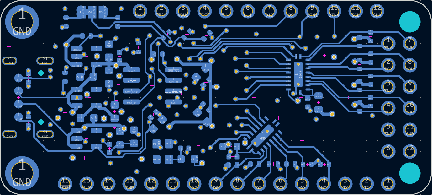 You can see the two level shifters on the right side of the board connecting to pin 4-9, as well as handling the PMOD connector. I am a really big fan of this level shifter. It's bidirectional, high speed, works for up and down translation, and is 8 bits wide. Internally it's basically just a bank of logical level FETs packaged together but that's fine.
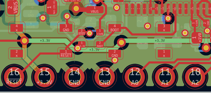 Based on my IO constraints I was only able to break out 3 pins capable of taking analog samples because for every analog pin it would take up 2 digital IO and I just couldn't spare them. Also, I am using the internal reference, which isn't particularly accurate and limits the measurement voltage to around 1V, sort of an ESP8266 vibe. There is obviously room for improvement here, and sometime I want to take another look at in future revisions of the board.