0%
0%
The Crystal Board
Affordable AND useful digital logic design. Finally.
 Chris
ChrisBecome a Hackaday.io member
Already have an account? Log in.
Just one more thing
To make the experience fit your profile, pick a username and tell us what interests you.
Pick an awesome username
hackaday.io/
Your profile's URL: hackaday.io/username. Max 25 alphanumeric characters.
Pick a few interests
Projects that share your interests
People that share your interests


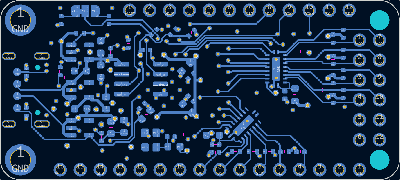 You can see the two level shifters on the right side of the board connecting to pin 4-9, as well as handling the PMOD connector. I am a really big fan of this level shifter. It's bidirectional, high speed, works for up and down translation, and is 8 bits wide. Internally it's basically just a bank of logical level FETs packaged together but that's fine.
 Based on my IO constraints I was only able to break out 3 pins capable of taking analog samples because for every analog pin it would take up 2 digital IO and I just couldn't spare them. Also, I am using the internal reference, which isn't particularly accurate and limits the measurement voltage to around 1V, sort of an ESP8266 vibe. There is obviously room for improvement here, and sometime I want to take another look at in future revisions of the board.


 Dylan Brophy
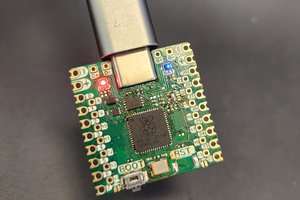
 2bluesc
 Casual Cyborg
Congrats!
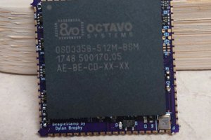
A $50 17K LUT (40K path) FPGA board with decent additions in a nice format sounds perfect.