 Guido - IW5ALZ
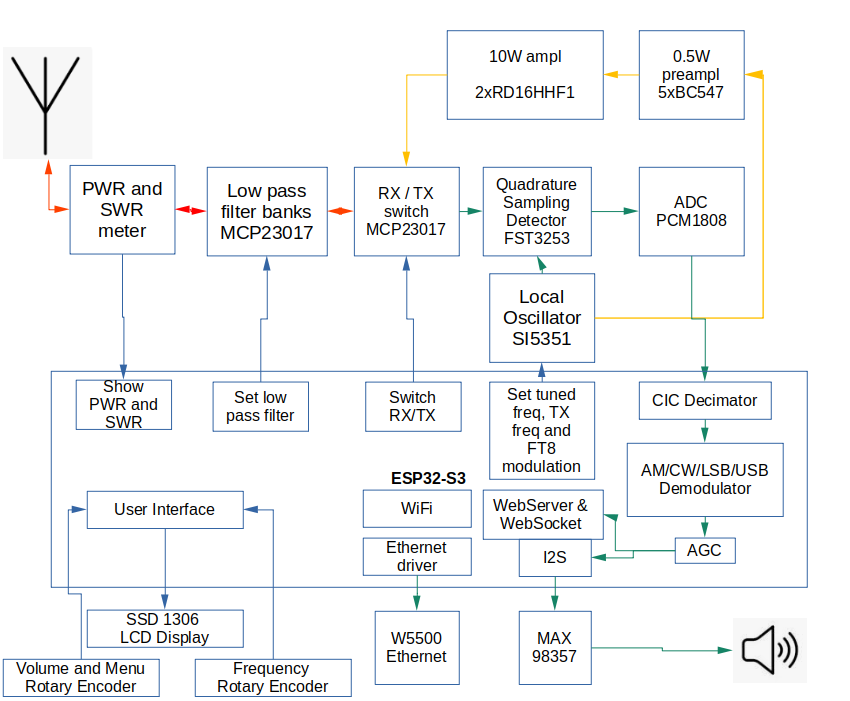
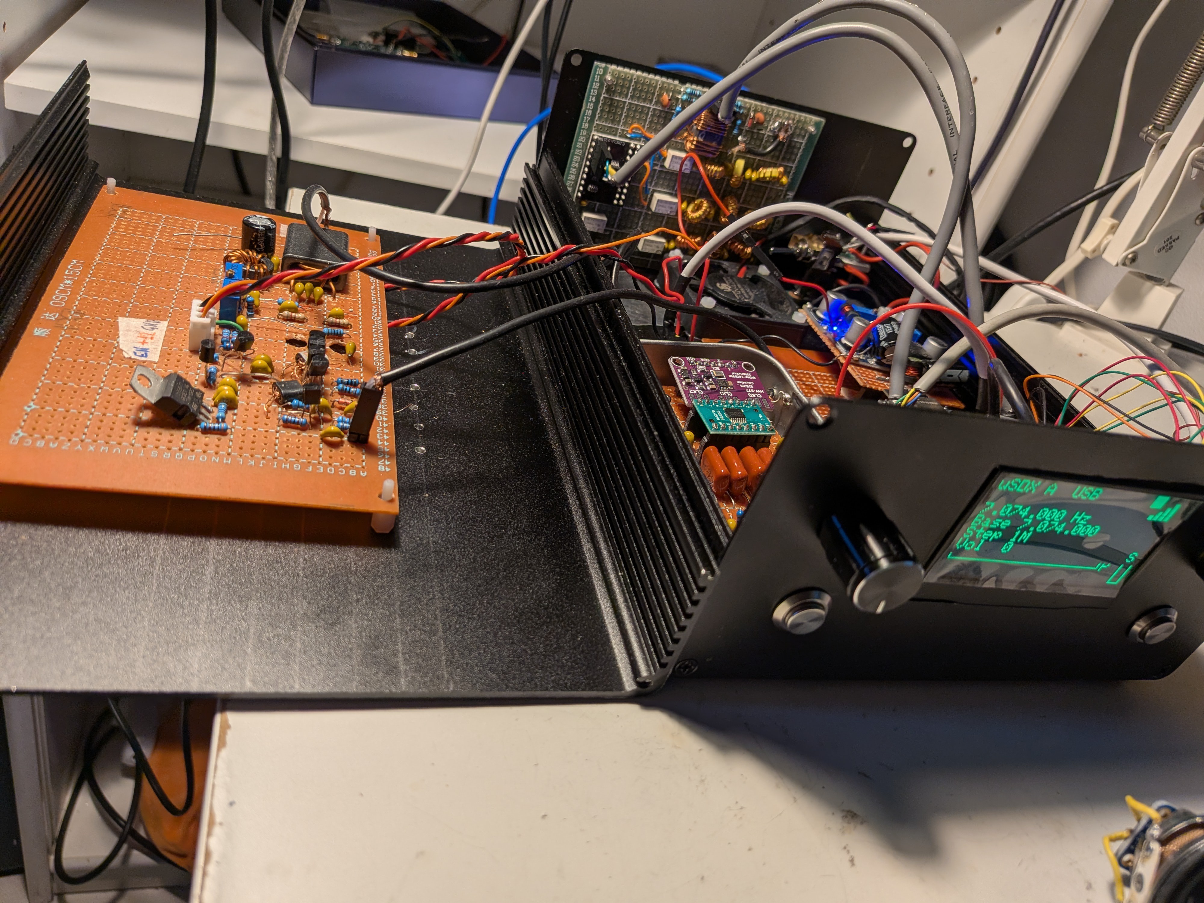
Overall Architecture
The design combines four key subsystems:
- RX: RF signal conditioning (Low pass filters and Tayloe QSD demodulator)
- TX: Power Amplifier, SWR and Power RF measurement
- digital control (ESP32 + MCP23017 filters switching + MAX98357 audio out)
- operator interface (encoders, display, buzzer)
Together these blocks form the front-end control and monitoring infrastructure of a modern QRP HF transceiver platform
1. Power and SWR Detection Circuit

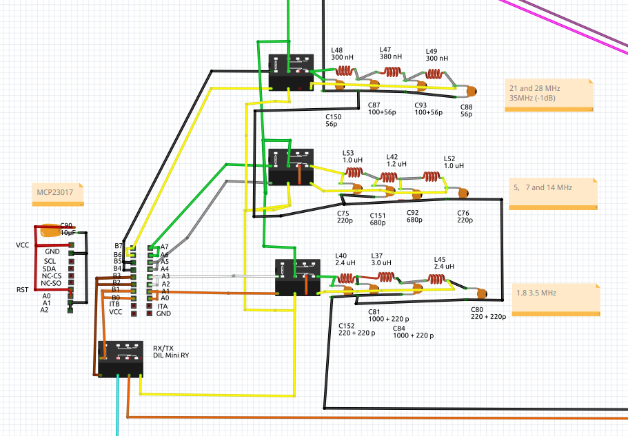
The antenna port feeds a directional coupler built around a binocular ferrite core (BN43-202).
This block samples the RF energy traveling in both directions on the transmission line.
Main functions:
- Sense forward power delivered to the antenna.
- Sense reflected power caused by impedance mismatch.
- Provide low-level RF samples for the measurement circuitry.
Two secondary windings on the binocular core couple a small fraction of the RF current from the transmission line. The resulting signals are rectified by detector diodes and converted to DC voltages proportional to the RF power.
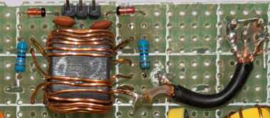
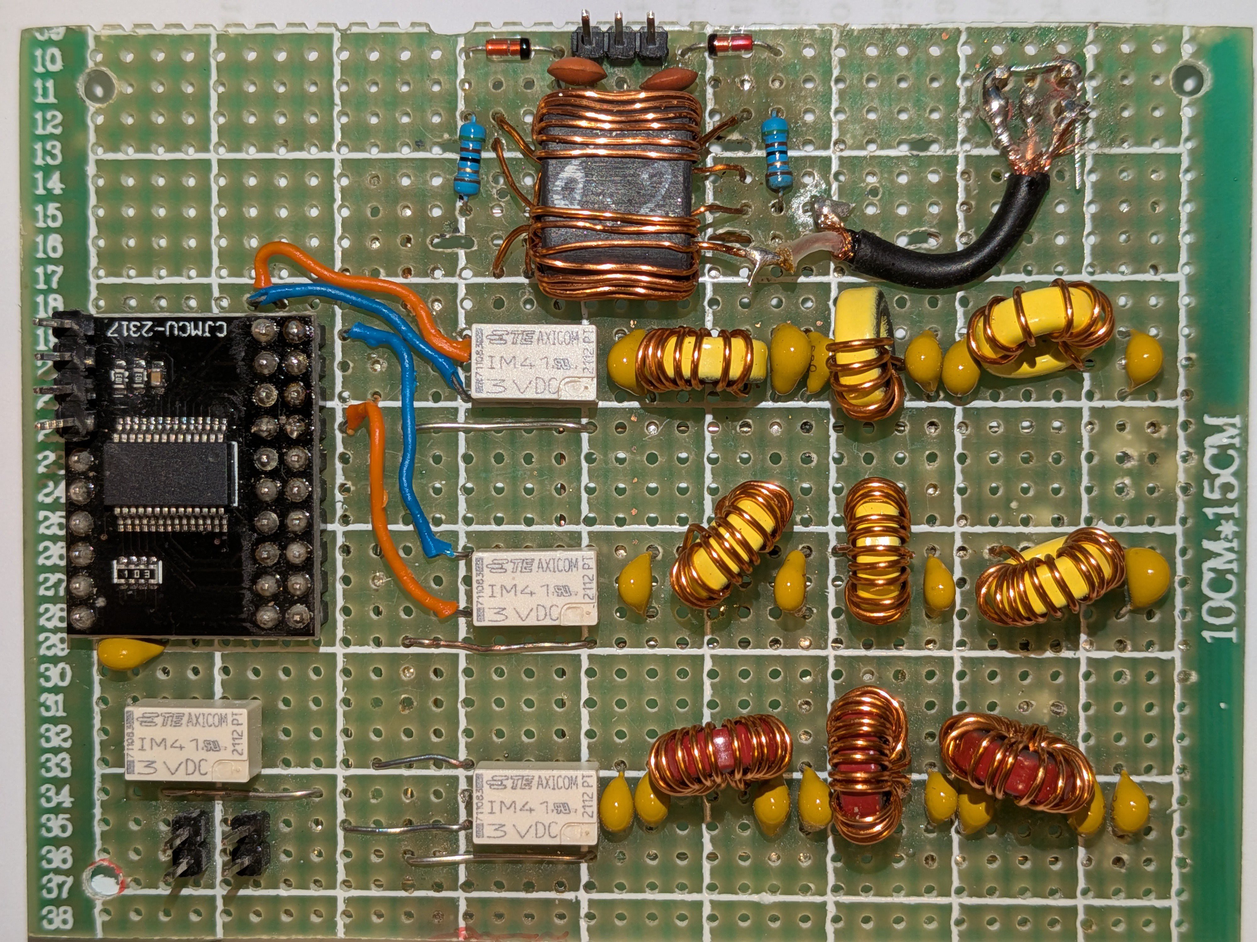
2. Low-Pass Filter Bank
The RF signal passes through a bank of relay-selected low-pass filters (LPF) designed to suppress harmonic emissions during transmission.
The filters cover the HF spectrum using three bands:
| Filter | Ham Bands Coverage | Frequency Range |
|---|---|---|
| LPF1 | 1.8 – 3.5 MHz | 0.1 - 5 MHz |
| LPF2 | 5 – 7 – 14 MHz | 5.1 - 10 MHz |
| LPF3 | 21 – 28 MHz | 10.1 - 30 MHz |
Each filter is a 7 poles Chebishev LC network built with toroidal inductors and RF capacitors.
Functions:
- Suppress transmitter harmonics
- Maintain regulatory spectral purity
- Provide good impedance matching in the passband
Latch Relays route the RF signal through the correct filter depending on the operating frequency selected by the controller.
The relay bank is driven by an I²C GPIO expander, the MCP23017.
This device expands the number of digital outputs available to the controller and performs several tasks:
- Drives filter-selection relays
- Controls RX/TX switching relays
- Simplifies wiring by using the I²C bus
Using an expander allows the microcontroller to manage many control lines while using only two pins (SDA and SCL).
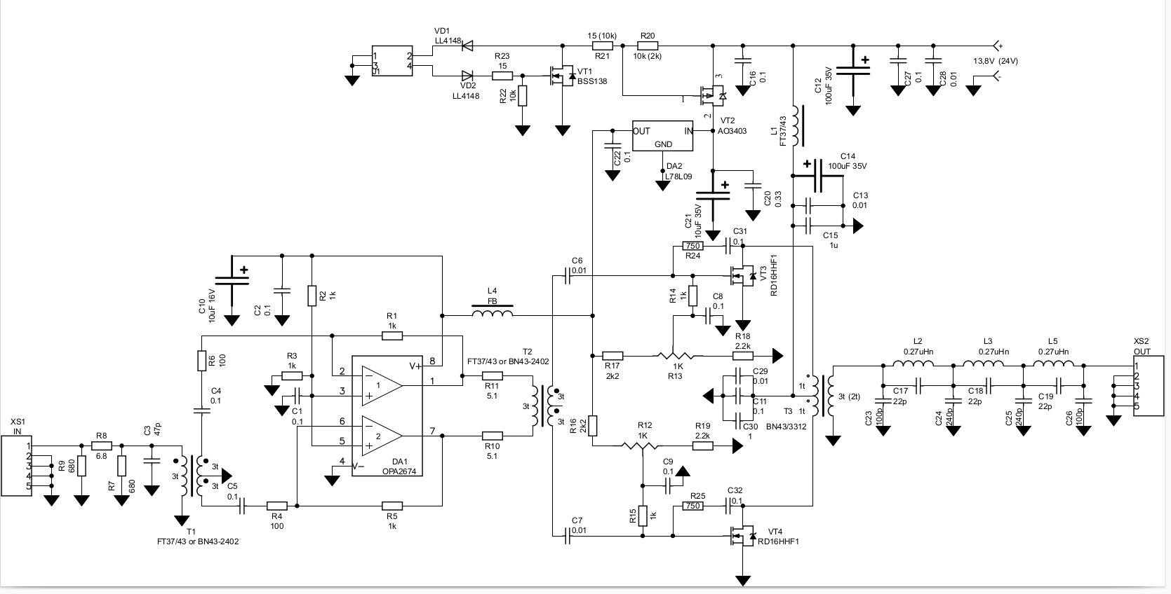
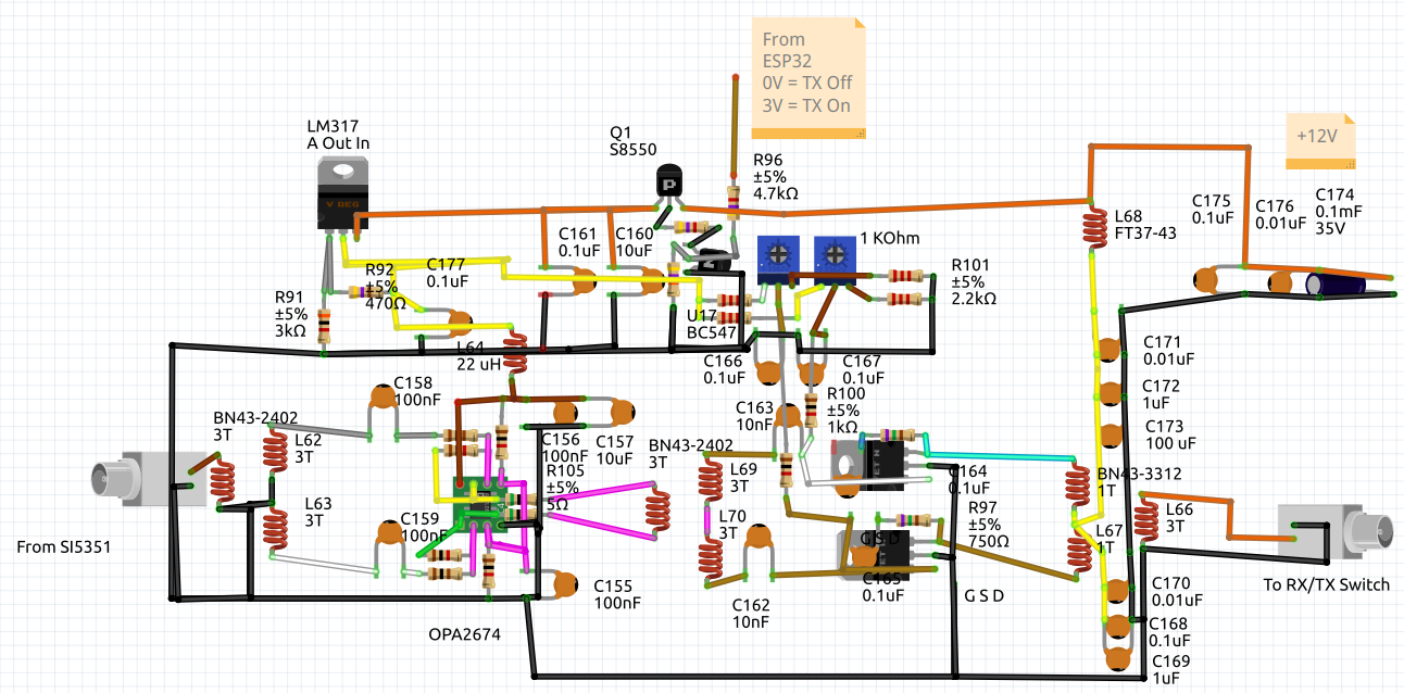
3. RF Power Amplifier Interface
The filtered RF signal connects to the RF power amplifier stage.
This block represents the connection point between the low-level RF system and the final amplifier.
Key roles:
- Deliver clean RF drive to the PA
- Route the transmit signal through the filter bank
- Return the received RF path toward the receiver
Proper impedance control (50 Ω) throughout this section is essential to minimize insertion loss and reflections.
For a complete description, please see my project: 1-30 MHz 0.5-1W (up to 10W) class C amplifier
4. Microcontroller Control System
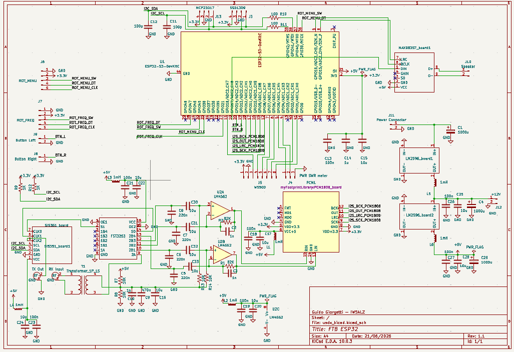
The central controller is an ESP32 microcontroller board.
It manages:
- the RF control logic
- the Digital Signal processing
- the user interface
- WiFi or Ethernet communication
Responsibilities include:
- Selecting the appropriate low-pass filter
- Reading SWR and power measurements
- Managing RX/TX switching
- Driving the display
- Handling user input from rotary encoders and buttons
The ESP32-S3 provides significant processing capability and built-in peripherals, making it well suited for digital control of RF equipment.
SDR Functionalities:
- LSB, USB, CW, AM Demodulation
- IQ Processing: DC removal
- Phase and amplitude correction
- CIC decimation filters
- downsample ADC IQ data to audio rates
- Hilbert transform for SSB demodulation
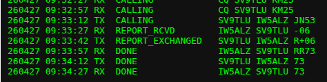
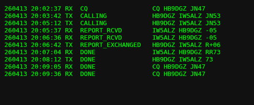
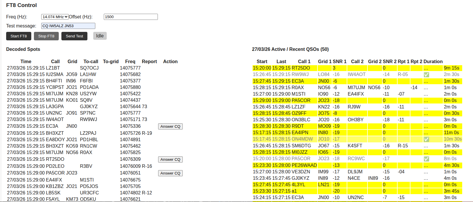
- FT8
- integrated FT8 encoding
- FT8 decoding happens by an embedded FT8 decoder. See also https://github.com/guido57/ESP32_ft8_lib
- QSO management (CQ / Answer)
- others QSOs view
5. User Interface
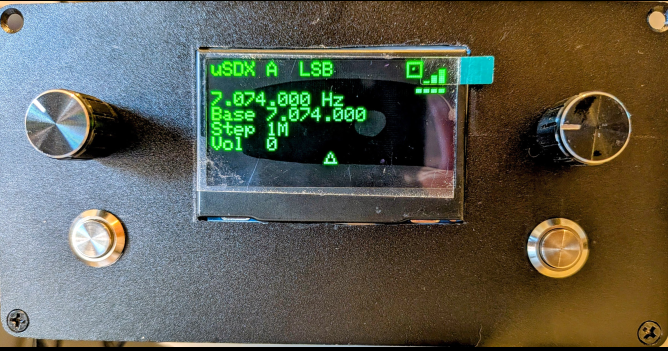
The interface allows the operator to control and monitor the system.
Main elements include:
- Frequency rotary encoder (on the right) for tuning
- Volume rotary encoder (on the left)
- Menu rotary encoder for configuration
- Push buttons...
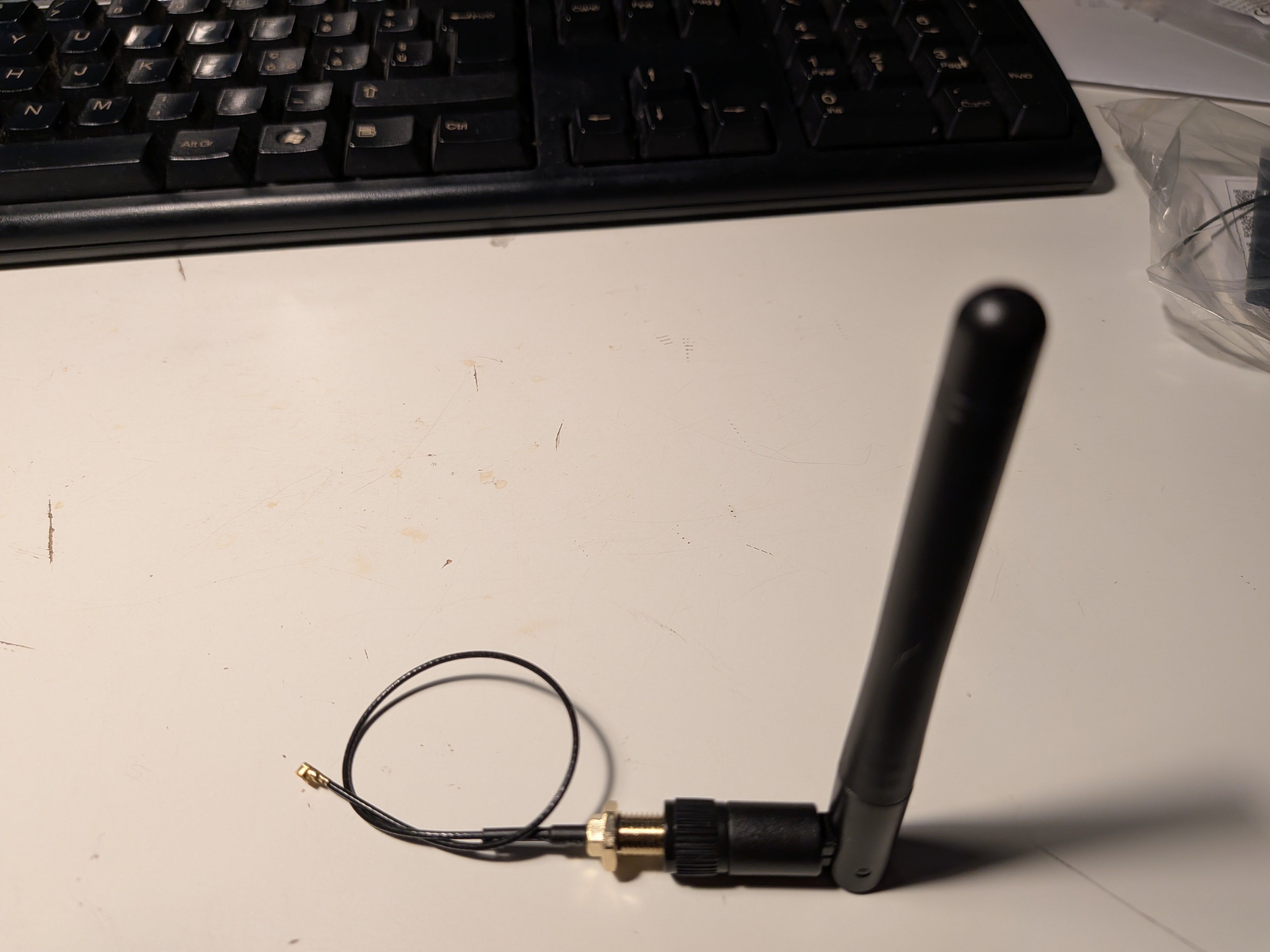

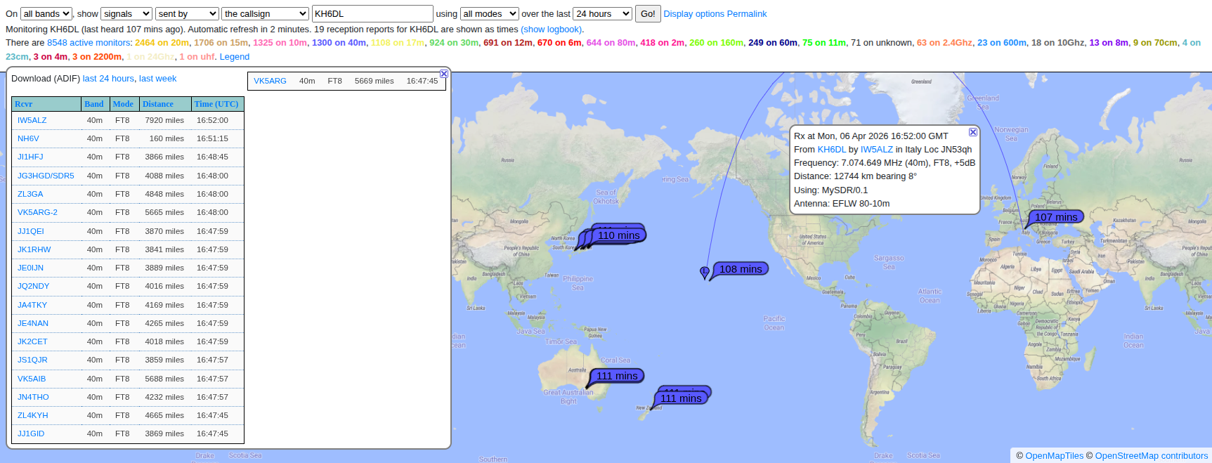 My antenna is nothing special as it's located at about 6 meters from the ground, between some buildings. Therefore I think my receiver is not so bad!
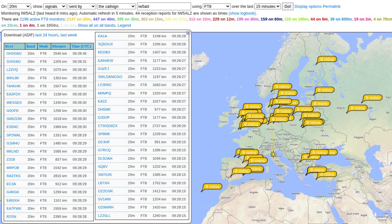
 drcyberg
 Sagar 001
 Daphne
 tshen2