Dariush Salami
-
Adding a Hardware Power Switch to the SensWear Main Board
08/28/2026 at 20:53 • 0 commentsWearable prototypes need a power state that is obvious and deterministic. A firmware-controlled shutdown or ship mode is useful, but it is not quite the same as moving a switch and knowing that the downstream system rails are isolated from their normal power source.
![]()
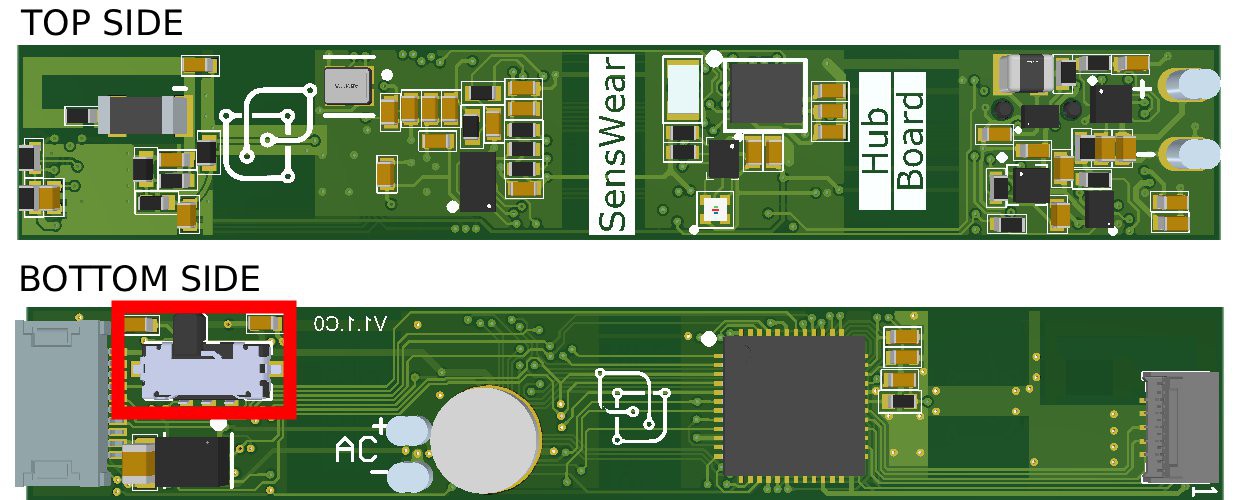
For revision C0 of the SensWear main board, we added that physical control: SW1, an ALPS Alpine SSAJ110100 latching slide switch. The interesting part is that the switch does not carry the board's operating current. Instead, it controls a pair of power MOSFETs that connect or isolate the main system rail.
Where the switch sits in the power path
SensWear uses a TI BQ25180 (U4) as its single-cell charger and power-path manager. Its SYS output can be supplied from the charging input or the LiPo cell. In the previous board revision, that output fed the rest of the board directly. In C0, the path is now:
V_SYS supplies the TPS62840 1.8 V regulator (U3) used by the main logic and the TPSM831021 sensor regulator (U6). Isolating V_SYS therefore removes input power from the MCU/logic and sensor power domains instead of asking firmware to shut each load down individually.
What happens in each switch state
The common terminal of SW1 is connected to both gates of T1, a TI CSD75207W15 dual P-channel MOSFET. The two MOSFETs are connected back-to-back with a common source.
SW1 electrical connection MOSFET gate condition Result Common connected to pin 1 Gates tied to the common-source node, so VGS is approximately 0 V Both MOSFETs are off and V_SYS is isolated Common connected to pin 2 Gates pulled toward ground through R5 VGS is negative, both MOSFETs turn on, and SYS feeds V_SYS Using two MOSFETs back-to-back matters. A single MOSFET still has a body diode, which can leave an unintended current path when the device is off. The opposing body diodes in T1 block current in both directions when the gates are tied to the source. This also reduces the opportunity for a downstream supply or connected module to back-power the charger-side SYS node.
When on, the MOSFET pair provides a low-resistance power path. TI specifies a maximum drain-to-drain on-resistance of 54 mΩ at VGS = -4.5 V, so the mechanical switch can remain a tiny signal-level part while T1 carries the actual system current.
The components added around the switch
The C0 change adds exactly four new designators:
- SW1 - ALPS Alpine SSAJ110100, a low-profile, latching SPDT slide switch mounted on the bottom side of the flexible main board. It is rated for 10 mA at 5 V, which is another reason not to place it directly in series with the system load.
- T1 - TI CSD75207W15, a dual common-source P-channel MOSFET. It forms the high-side, bidirectional-isolating load switch between U4.SYS and V_SYS.
- R10 - 1 MΩ from the common gate node to the MOSFETs' common source. It prevents the gates from floating and biases the pair toward the off state when there is no gate pull-down.
- R5 - 22 kΩ between the on-side switch contact and ground. When selected, it pulls the gates low and turns the P-channel pair on. Together with R10, it puts the gate at about 2.15% of the source voltage and draws only a few microamps of static bias current. This is a gate-bias network, not a debounce circuit; no debounce capacitor was added.
This arrangement lets us use a mechanically small switch suitable for a thin wearable board without routing the full load current through its contacts.
Hardware off, with one deliberate boundary
The new switch is independent of the MCU and the existing PWR_KILL/ship-mode control. It works even when firmware is stuck or has not started.
However, “off” here means that the downstream system rail is disconnected. SW1 is located after the charger's SYS output, so it does not physically disconnect the LiPo cell from the BQ25180 charger or the BQ27427 fuel gauge. The battery-management side remains connected, and the charging input can still reach the charger while the main logic and sensor rails are isolated.
There is also a firmware tradeoff: the switch removes power immediately and does not first send a shutdown request to the MCU. Any data logging or non-volatile-memory write must therefore tolerate power being removed at an arbitrary moment.
What we will verify on the C0 hardware
The schematic, PCB layout, BOM, pick-and-place file, and manufacturing outputs have been updated for C0. This log describes the design and its intended operation, not completed bench characterization. The generated PCB check reports no shorts or unrouted connections, but it still contains one bottom-silkscreen-to-board-edge clearance violation unrelated to the switch circuit, so we are not calling the revision fully validated yet.
The next useful measurements on assembled boards are:
- V_SYS and 1V8 rise/fall behavior when switching on and off;
- off-state current at the battery, including the charger and fuel-gauge overhead that remains upstream;
- reverse leakage or back-powering from attached modules and debug connections;
- voltage drop and temperature across T1 under representative loads;
- behavior when switching off during an external-memory write; and
- actuator access and mechanical clearance in the intended enclosures.
The design change is available in the SensWear hardware repository and in the C0 switch commit. Component details are in the SSAJ110100 product page, the CSD75207W15 data sheet, and the BQ25180 data sheet.
For other wearable developers: do you prefer an immediate hardware power cut, a soft shutdown followed by a load switch, or both?
-
SensWear in the Classroom: Smart-Ring Gesture Recognition at Aalto
08/13/2026 at 15:01 • 0 commentsSensWear was recently used as the project platform for Introduction to AI-Enabled Wearable Technologies at Aalto University Summer School in Espoo, Finland.
During the course, students explored the wearable-AI pipeline using SensWear’s smart-ring form factor: capturing raw IMU motion data, visualising and processing signals, collecting gesture examples, and developing a basic gesture-recognition model.
The video below captures the hands-on prototyping sessions and collaborative workflow. The course also provided a valuable real-world test of SensWear’s modular hardware, raw-data access, and suitability for teaching and rapid wearable-AI prototyping.
- Hardware: SensWear smart-ring form factor
- Application: Gesture recognition
- Course: Aalto University Summer School, 10–21 August 2026
Next, we’ll use the lessons from these sessions to improve the platform’s tooling, documentation, and gesture-recognition workflow.
-
SensWear Platform Tour: From Modular Components to a Working Wearable
08/10/2026 at 11:39 • 0 commentsIn this update, we’re taking a closer look at SensWear, our fully open-source, modular wearable platform, and showing how its components come together to create a functional wearable system.
The video introduces the complete hardware ecosystem:
- Smart-ring enclosure
- Debug board for programming and hardware bring-up
- Flat-flex connector
- Core hub board featuring the nRF54L15 BLE SoC and BHI360 IMU
- Touch daughter board
- PPG daughter board for heart rate and SpO₂ measurements
- Vibration daughter board for haptic feedback
- Temperature daughter board for body-temperature sensing
We also demonstrate the platform’s assembly workflow: connecting the debug board to the hub, inserting and removing the hub through the ring enclosure’s open edge, adding the touch module, and serially connecting the PPG and temperature daughter boards.
SensWear is designed to make wearable development easier to build, modify, and extend. The same core platform can support different sensors, interaction methods, and form factors without requiring a completely new device for every application.
We’re continuing to refine the hardware and prepare the project for its Crowd Supply campaign. Follow this project for future development logs, technical details, and campaign updates: https://www.crowdsupply.com/sensera-technologies/senswear-wearable-dev-kit
-
Debug Board V2: No External J-Link Required
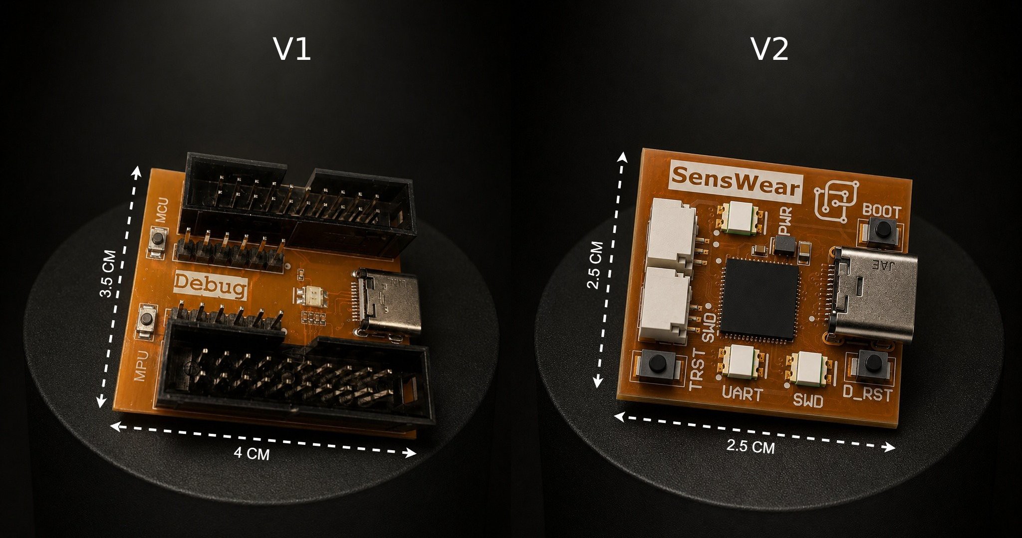
08/06/2026 at 15:53 • 0 commentsThe first SensWear debug board combined an FT232RL USB-to-UART bridge with two external J-Link headers. It worked for development, but required a separate J-Link probe and occupied a relatively large 40 × 35 mm PCB.
![]()
The second revision integrates an RP2354A-based Pico-style debugger directly onto the board. It is designed to provide MCU SWD programming/debugging and UART access through USB-C, with dedicated SWD and UART activity LEDs. We also added BOOT, target-reset and debugger-reset buttons, 3-pin SWD/UART breakout connectors, and dedicated power regulation and signal buffering.
Despite the added functionality, the board measures only 25 × 25 mm, about 55% less PCB area than V1. More importantly, the complete programming, debugging and serial-console workflow no longer depends on an external J-Link.
We have now assembled and successfully tested the new board. The hardware design, manufacturing outputs, firmware and the rest of the SensWear stack are openly available through the SensWear GitHub organization, including the hardware repository.
SensWear: An Open Source Modular Wearable Platform
An open source and modular wearable hardware platform for researchers and makers, building flexible sensing and edge AI.