 Zduka
ZdukaAfter xmas 2025 I was in a good shape. I have delivered two working RCKids to my betatesters and they were inseparable from the device. I have also experienced my personal variant of the Tetris effect - once I made the tetris game for the device, development grinded to a halt since I spent most of my free time "betatesting" myself. And a few more clouds popped on the sky relatively soon:
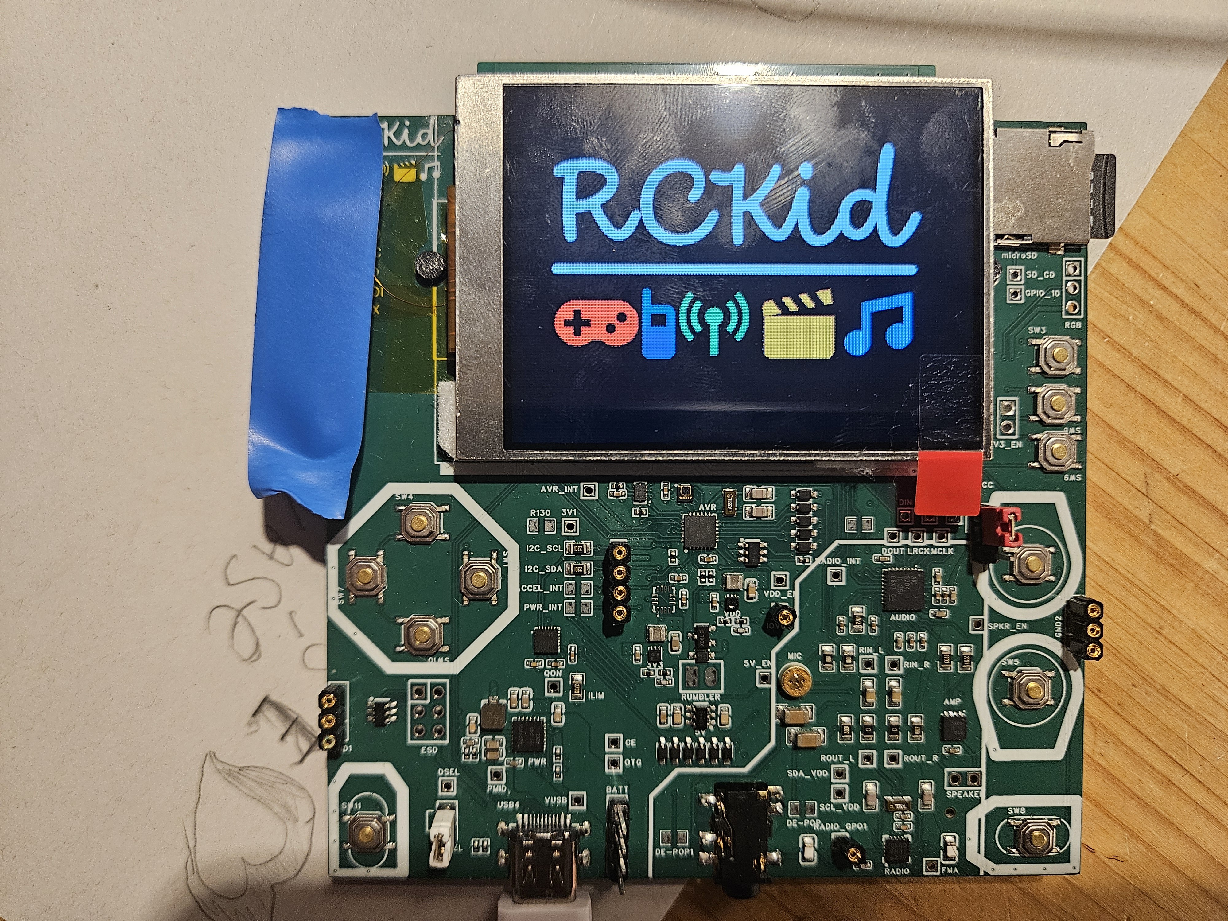
My kid's devices actually did not have the cartridges. I should really say did not have *removable* cartridges, as the cartridge was still inside the device, just the 3d printed cover did not have the hole necessary for its removal. I have realized that the precision machined pins were all too easy to be destroyed (bent) by normal use. 4y old would destroy that in a matter of minutes.
When you started charging the device via USB, it became unusable as the buttons went all crazy with phantom presses. It took me a while to figure out what went wrong, but here it is: Through most of the revisions, I kept basic structure that I used already in my previous mp3 player project - the big chip (RP2340, RPi Zero, etc.) does almost all the hard stuff, but there is always ATTiny on the side, which is always powered on, manages the power, buttons and other important (or simple tasks). The ATTiny communicates with the big chip via I2C. And one of its jobs is to measure the voltage for a poor man's battery gauge. Normally you would need a pin an ADC for this. But all my pins were used. Luckily there is a really neat way to measure VCC with ATTiny without wasting a pin - you tell the ADC to measure internal reference instead. The ADC runs off the VCC, how much it measures can be converted to the VCC value. This seemed perfect - I do not need a DC-DC converter or LDO for the always on ATTiny, I do not waste a pin, and I do not have to turn it on or off. I2C is also fine, as it will be pulled-up externally to 3V3 and the AVR only even pulls low. Since I did not support going VCC below 3.3V at the time anyways, this seemed perfect. Unfortunately, when AVR is powered from 5V, the 3v3 is just at the edge of low to high input transition, and more often than not, the I2C IO was misbehaving because of that.
I did not have any more displays and had to order more. As I had big plans, I just repeated my previous order from AliExpress, just this time with 20 units and waited. Also, Raspberry Pi has created the RP2350 - much better chip (M33 vs M0, 2x memory for 512KB, more pio, more DMA, etc. And crucially ability to have external RAM - imagine if my cartridges could support external RAM next to the flash as well. But I knew from my past that feature creep is real danger, and so I resisted, almost tearfully. Then the new displays arrived.
Same display, same hand solderable connector, same everything, including the URL from which I ordered. But none of the displays worked. But none of them worked. Frustrated, I tried everything, and then I realized that on the display back, literally in a smallprint, there was a teeny tiny difference, my old 2 displays ended with 8, this one ended with 16. You probably guessed it, they were hardwired to 16 parallel 8080 MCU interface. The display I have been using so far was no longer produced.
A sane person would be depressed at this point. I was ecstatic - this was my justification for going with RP2350 without giving in to the peer pressure. See RP2350 had one more huge advantage - the B variant with a few more GPIOs. Now if I get this chip, I will have enough pins to drive the 16bit display:) No other way. Except of course, I also started learning about DFM and figured out that if I have QFN chips assembled already, I can also throw in a nice display FPC connector for almost no extra cost. And I could get FPC connector 8bit display, but pssst:) RP2350 is the future!
And indeed it was! I redesigned everything - but most importantly I have added 1.5mm of thickness to the device which is barely visible, but allowed me to put components *under* the display too (the RP2350 is *bigger*) and with this extra room for placement & layout and extra pins to use, I decided to go with proper sound via I2S audio codec. Feature creep came back with vengeance though - audio codecs are amazing! So the microphone switched from PDM to electret and I used the audio codec. And since I had some free audio inputs, I decided to also throw in an FM radio. I have of course fixed the power problem with a fancy new PMIC chip that I read in one of its datasheets (it came with 5) always regulates the system voltage above a certain threshold via integrated boost controller. I also changed the cartridge connector - it now uses daughterboard and antenna springs for connection with the cartridge being just a PCB with gold fingers (they are actually HASL lead free fingers to be precise, but they work).
Measure twice, cut once
Or really verify semantics & PCB 5 times, do automated assembly once. I have also realized that the three revisions I did in with the mkII version were completely unnecessary if only I had a board that I can solder and desolder things myself with enough test points. I could not do this - the device is small, and all the passives were 0402, way too small for me to handle. So this time, instead of going to the desired form factor first, I have created a 10x10cm development board that had everything I wanted to have in mkIII surrounded by redundant traces, test points and large 0805 components that I knew from mark I with RPi Zero are at the edge of my skill.
Except of *all* the connections, I completely forgot to use RUN pin of the RP2350 in the schematics, hence DRC did not pick it up, and this enormously vital pin (if left unconnected, RP2350 will not boot basically) was left without even a testpoint. Luckily I know a guy who is next level in soldering and he attached a teeny tiny wire to the barely visible QFN pad on the side without bridging the rest. I had my dev board!
Don't trust components with multiple datasheets
At least if you are amateur like me. Turned out that the PMIC chip did not do what I wanted from it (won't regulate VSYS when powered from batt), and the audio codec did not work with the microphone - I went again into overdrive and added not just one microphone, but a second one via the headphone jack as well because why not. 2 microphones sharing same micbias driver, bad idea. Both components came with multiple hudndred+ page datasheets, which I did read, but missed this vital information.
But now the devboard with its many testpoints paid off. I have ordered simple breadboard converters populated with NAU88C22 audio coded that I found, which looked much better - worse audio, but integrated speaker driver as well. Most importantly the datasheet looked simple.
So I ended up with the following architecture (in beautiful handcrafted ASCII art form):
And it worked! This time I had 4 devices for xmas:-) I have also tried 3d printing services, mainly because the Internet said that transparent cases can be made this way and I saw my son being so very excited about a see-through xbox controller he saw in a shop. I have also experimented with full color silkscreens. For normal use they are rather expensive by my standards, but I got some for free, thanks to JLCPCB. I must admit the cases turned out amazingly well:
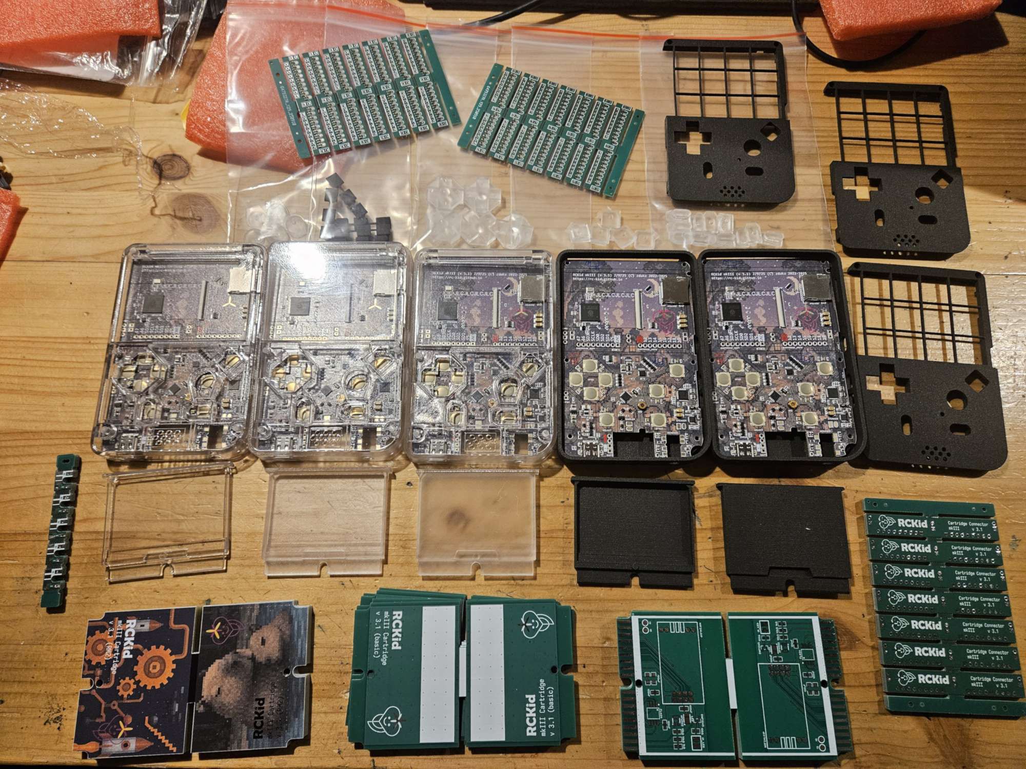
In the end, I do not think I will keep them for the main case - it is mostly obscured by the components, battery and display and I do not need the ENIG surface they require. On the other hand, the cartridges with full color silk-screen look absolutely amazing - and they can use the ENIG finish for the cartridge connector.
My parting comment for today: SLA resin prints are *not* thermoplastics, so using your soldering iron to melt in it threaded inserts for assembly will break them. I learned it the hard way.
Up next: Audio system (because analog circuits scare me:)
Discussions
Become a Hackaday.io Member
Create an account to leave a comment. Already have an account? Log In.