 Paul Horsfall
As mentioned in the introduction, I've been working on a breakout PCB to facilitate experimenting with the family of ADCs I'm considering using for this project. The board supports the 10 bit / 20 Msps AD9204 that I expect I'll use initially, but can also work with a range of pin-compatible parts, which I may use to experiment with 12 or 14 bit parts.
Here's a diagram that gives a high-level view of the design:
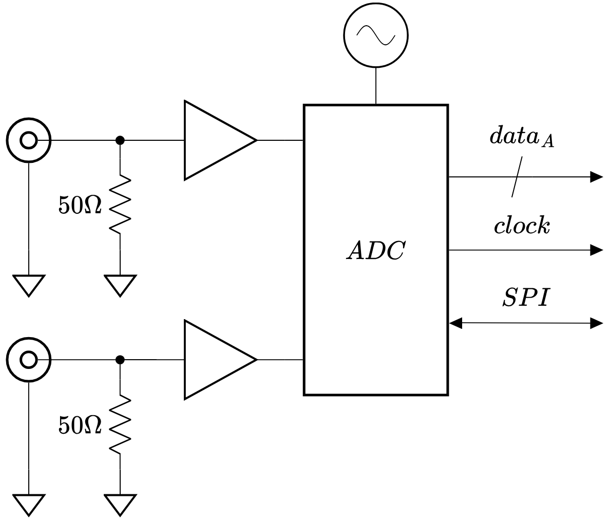
There are two 50 ohm inputs, each driving one of the two ADC inputs through a buffer. A crystal oscillator provides a low jitter clock to drive the ADC. (Though not shown in the diagram, I also have a couple of options for driving the ADC from an external clock.) One of the ADC's two data and clock outputs is made available via pin headers. (I choose to expose only a single output channel because I couldn't conveniently connect both channels to my FPGA breakout board. However, the ADC is capable of multiplexing both channels onto a single output, so I expect to still be able to make use of both channels.) The ADC's SPI interface is also available on pin headers.
The board was laid out in KiCAD and manufactured by JLCPCB. Here's a picture of an unpopulated board:
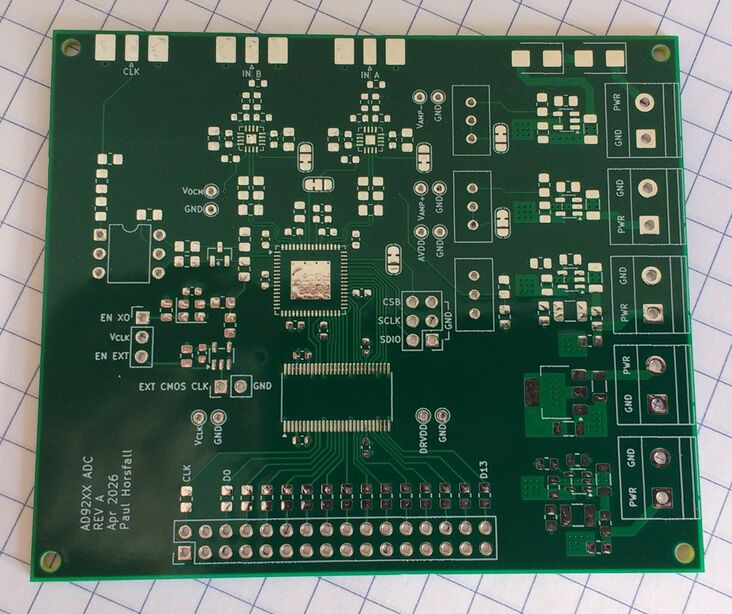
The next step is to attempt assembly...
Discussions
Become a Hackaday.io Member
Create an account to leave a comment. Already have an account? Log In.