 Victor Zhang | TJHXPCB
Overview
This project documents the design and development of a compact 200W Brushless DC (BLDC) motor controller using the Texas Instruments DRV8301 gate driver and STMicroelectronics STM32F303 microcontroller. The controller implements Field-Oriented Control (FOC) for smooth torque delivery across the full speed range — targeting robotics, industrial automation, and electric mobility applications requiring precise motor management in a small form factor.
The DRV8301 integrates a dual-channel bootstrapped gate driver, overcurrent protection, and a dual SPI-configurable current sense amplifier — significantly reducing external component count compared to discrete gate driver implementations. The STM32F303's hardware floating-point unit and dedicated motor control timers make it well-suited for real-time FOC computation at 20kHz PWM frequency.
Design Goals
- Continuous output power: 200W
- Operating voltage: 12V – 48V DC bus
- Peak phase current: 20A
- PWM switching frequency: 20kHz
- Control loop: Field-Oriented Control (FOC)   with Space Vector Modulation (SVM)
- Protection: Overcurrent / Overvoltage /   Undervoltage / Overtemperature
- Communication: CAN + UART
- Form factor: 70mm × 55mm 4-layer PCB
Hardware Architecture
Power Stage
The three-phase inverter uses six N-channel MOSFETs arranged in a standard H-bridge topology. The DRV8301 drives all six gates with adjustable dead-time insertion (50ns – 400ns via SPI) to prevent shoot-through at high switching frequencies. Bootstrap capacitors are sized for 48V operation with a 10% duty cycle minimum gate charge requirement.
Gate resistors are individually tunable per high-side and low-side switches — allowing independent control of turn-on and turn-off slew rates to balance switching loss against EMI. A common-mode choke on the DC bus input reduces conducted emissions from the high-frequency switching node.
Current Sensing
Phase current is measured using two shunt resistors on the low-side of phases A and B, with phase C current reconstructed by Kirchhoff's current law. The DRV8301's internal current sense amplifiers (gain selectable: 10x / 20x / 40x / 80x via SPI) feed directly into the STM32F303's 12-bit ADC — eliminating the need for external instrumentation amplifiers and simplifying the analog front-end layout.
ADC sampling is synchronized to the PWM center point via the STM32 advanced timer trigger — ensuring current samples are taken at the point of minimum switching noise, which is critical for stable FOC operation at low speeds.
Microcontroller and Control Loop
The STM32F303's 72MHz Cortex-M4F core runs the complete FOC algorithm including Clarke/Park transforms, PI current controllers, inverse Park transform, and Space Vector Modulation — all in fixed-point arithmetic on the FPU within a 50µs interrupt service routine. The hardware encoder interface captures quadrature encoder signals up to 4MHz for rotor position feedback.
CAN communication (125kbps – 1Mbps) handles command input and status telemetry in multi-axis systems. A secondary UART interface supports configuration and real-time data logging during development.
PCB Design Considerations
Laying out a mixed-signal power electronics board at this power level requires careful attention to current loop geometry, thermal management, and analog signal isolation.
The 4-layer stackup separates high-current power planes from the sensitive analog and digital signal layers:
Layer 1: Signal (MCU, gate drive signals, SPI, CAN)
Layer 2: Ground plane (solid, uninterrupted)
Layer 3: Power plane (12V-48V, PWM bridge)
Layer 4: Signal (current sense, analog, encoder)
The high-current switching loop — DC bus capacitor, MOSFET drain, source, and shunt resistor — is kept as small as possible to minimize parasitic inductance. Stray inductance in this loop directly causes voltage spikes on the MOSFET drain at turn-off, which can exceed device ratings if the loop area is not minimized.
Gate...
Read more »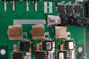
 Kai Yin
 Marcos