electronicsworkshops

Introduction
Modern electronic systems require stable and efficient power supplies to ensure reliable operation. Whether you're powering embedded systems, robotics, IoT devices, or industrial electronics, converting a higher DC voltage into a regulated lower voltage is one of the most common design challenges.
The SY8205 synchronous buck converter is an excellent solution for high-current, high-efficiency voltage conversion. It offers excellent efficiency, compact PCB design, and minimal external components, making it ideal for battery-powered and embedded applications.
In this article, we'll explore the design, working principle, PCB implementation, and applications of a DC-DC Step-Down Voltage Regulator Using SY8205.
For Full Project:
https://electronicsworkshops.com/dc-dc-step-down-voltage-regulator-using-sy8205/
For Best Electronics Calculator:
https://numericalcalculator.com/
What is a DC-DC Step-Down Converter?
A DC-DC step-down converter, also known as a Buck Converter, converts a higher DC input voltage into a lower regulated output voltage while maintaining high efficiency.
Unlike traditional linear regulators, switching regulators waste very little power as heat.
Why Choose the SY8205?
The SY8205 is a high-performance synchronous buck converter designed for compact and efficient power supply applications.
Key Features
Wide input voltage range
High output current capability
Integrated MOSFETs
High conversion efficiency
Fixed switching frequency
Short-circuit protection
Thermal shutdown protection
Over-current protection
Soft-start functionality
Compact SOP package
These features simplify PCB design while reducing component count and improving reliability.
How the SY8205 Works
The SY8205 operates using Pulse Width Modulation (PWM) to regulate the output voltage.
Its operation consists of four main stages:
1. Input Filtering
The input capacitor filters supply noise and provides stable power to the regulator.
2. Switching Stage
The internal MOSFET switches rapidly at high frequency, transferring energy to the inductor.
3. Energy Storage
The inductor stores energy while the switch is ON and releases it when the switch turns OFF.
4. Output Filtering
The output capacitor smooths the switching waveform into a clean, stable DC voltage.
This switching mechanism minimizes power loss and maximizes efficiency.
Circuit Diagram
The circuit shown is a DC-DC step-down (buck) voltage regulator based on the SY8205FCC synchronous buck converter IC, designed to convert a higher DC input voltage into a stable lower output voltage with high efficiency. The input power is supplied through the XT30PW-M connector (CN1) and is filtered by a combination of bulk electrolytic capacitors (C7, C8, U2, and U3) and ceramic capacitors (C6) to reduce voltage ripple and suppress high-frequency noise before reaching the regulator IC. The SY8205FCC (U1) serves as the main switching controller, while the bootstrap capacitor C1 supports the internal high-side MOSFET operation. The switching output from the LX pin passes through the 6.8 µH inductor (L1), which stores and releases energy during each switching cycle, producing a smooth DC output. The output voltage is further filtered using capacitors C4, C5, C9, and C10, ensuring a clean and stable supply for the connected load.
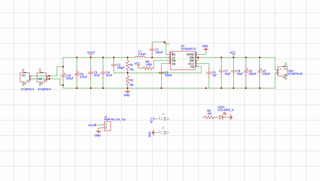
The output voltage regulation is achieved through the feedback network consisting of R1 (75 kΩ) and R2 (10 kΩ), which forms a voltage divider connected to the FB (Feedback) pin of the SY8205. This network continuously monitors the output voltage and allows the IC to adjust the switching duty cycle to maintain a constant regulated output despite variations in input voltage or load current. The R5-C3 network provides compensation and stability for the control loop, while C2 acts as a feed-forward capacitor to improve transient response and reduce output ripple. An XT30PW-F connector (U4/U5) and a 2-pin header (J1) provide...
Read more »
 Sagar 001
 Naman Chauhan