 Maxim Pavlov
PSU-EXT sits between an existing bench power supply and its load. It measures voltage and current and controls the output path with a relay. This update follows the development of its voltage measurement front end, from fixed converter settings to automatic range selection and programmable acquisition speed.
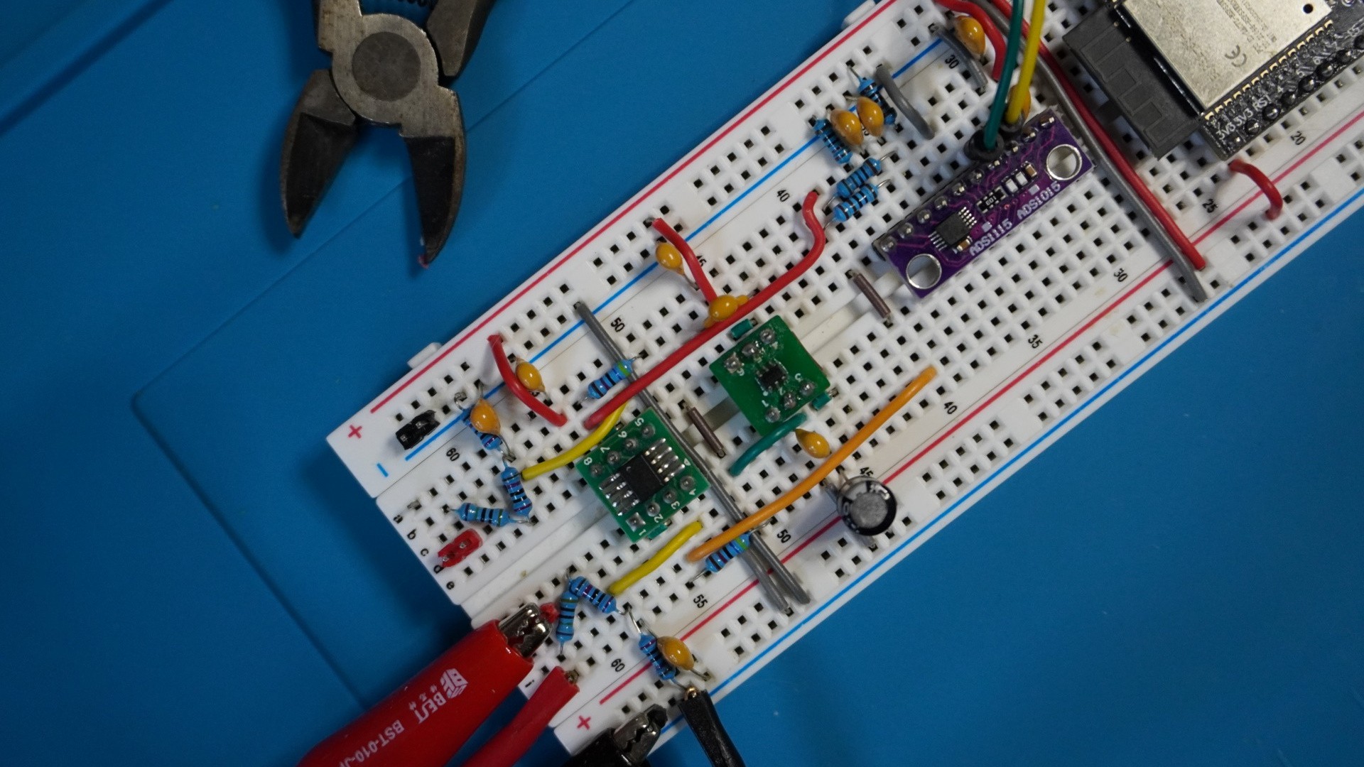
The existing design works with a fixed programmable gain amplifier (PGA) setting and a fixed analog-to-digital converter (ADC) rate. Its DC voltage accuracy is:
- ±(0.1% of reading + 2 mV) from 1 V to 24 V
- ±(0.5% of reading + 2 mV) below 1 V
That gives us a useful starting point. The next step is to use more of the ADS1115's capabilities: select a measurement range automatically and let the acquisition speed suit the task. Following that idea through the firmware led to two additions to the analog circuit: voltage buffers and a negative-rail output bias.
Making the Converter Settings Programmable
The ADS1115 has several full-scale input ranges. A smaller range gives a smaller voltage step per ADC count, which is useful when measuring low voltages. Autoranging lets the firmware select a narrow range for a small signal and move to a wider range as the signal rises.
The updated firmware uses three ranges: ±0.256 V, ±0.512 V, and ±2.048 V. These are voltages at the ADC input, after the voltage divider.
The range selection code moves one range at a time. Separate thresholds for moving up and down provide hysteresis, so a reading near a boundary does not repeatedly switch ranges. This excerpt comes from components/measure_svc/measure_prov_ads1115.c:
uint8_t index = current_index;
if ((index + 1U < ADS1115_RANGE_COUNT) &&
    (adc_voltage_u4 >= ADS_RANGES[index].hysteresis_top_u4)) {
    ++index;
} else if ((index > 0U) &&
    (adc_voltage_u4 <= ADS_RANGES[index].hysteresis_bottom_u4)) {
    --index;
}
*next_index = index;
Each input keeps its own range index. The firmware can therefore choose a range independently for each measured signal.
Acquisition speed is now programmable too. The driver accepts the ADS1115 rates of 8, 16, 32, 64, 128, 250, 475, and 860 samples per second. For example, these cases encode two rates into the configuration register:
case 128U:
    *bits = (uint16_t)0x04U << 5;
    return ESP_OK;
case 250U:
    *bits = (uint16_t)0x05U << 5;
    return ESP_OK;
These settings control the converter rate. The update rate for a complete set of measurements also depends on channel scanning and settling conversions.
The new Standard Commands for Programmable Instruments (SCPI) command exposes this setting to users:
| Command | Description |
| MEASure:ADC:RATE <SPS> | Set the ADC conversion rate in samples per second |
| MEASure:ADC:RATE? | Read the selected rate as an integer |
Following the Signal Back to the Divider
During development of the programmable-rate mode, changing the ADC rate also changed the voltage reading for a steady input. The current channel, driven by an INA240 current-sense amplifier, stayed stable in the same experiments. That difference pointed us toward the circuit driving the ADC.
Each voltage channel uses two 160 kΩ resistors above a 20 kΩ resistor. The nominal division ratio is 17:1. At a 30 V input, the divider produces about 1.765 V while drawing about 88 µA.
Rsource = 320 kΩ || 20 kΩ ≈ 18.8 kΩ
The ADS1115 uses a switched-capacitor input. Its input loading interacts with the resistance of the source driving it; The ADS1115 datasheet describes this behavior. The observed rate-dependent shift made source impedance a practical design consideration for the new operating modes.
Adding a Buffer
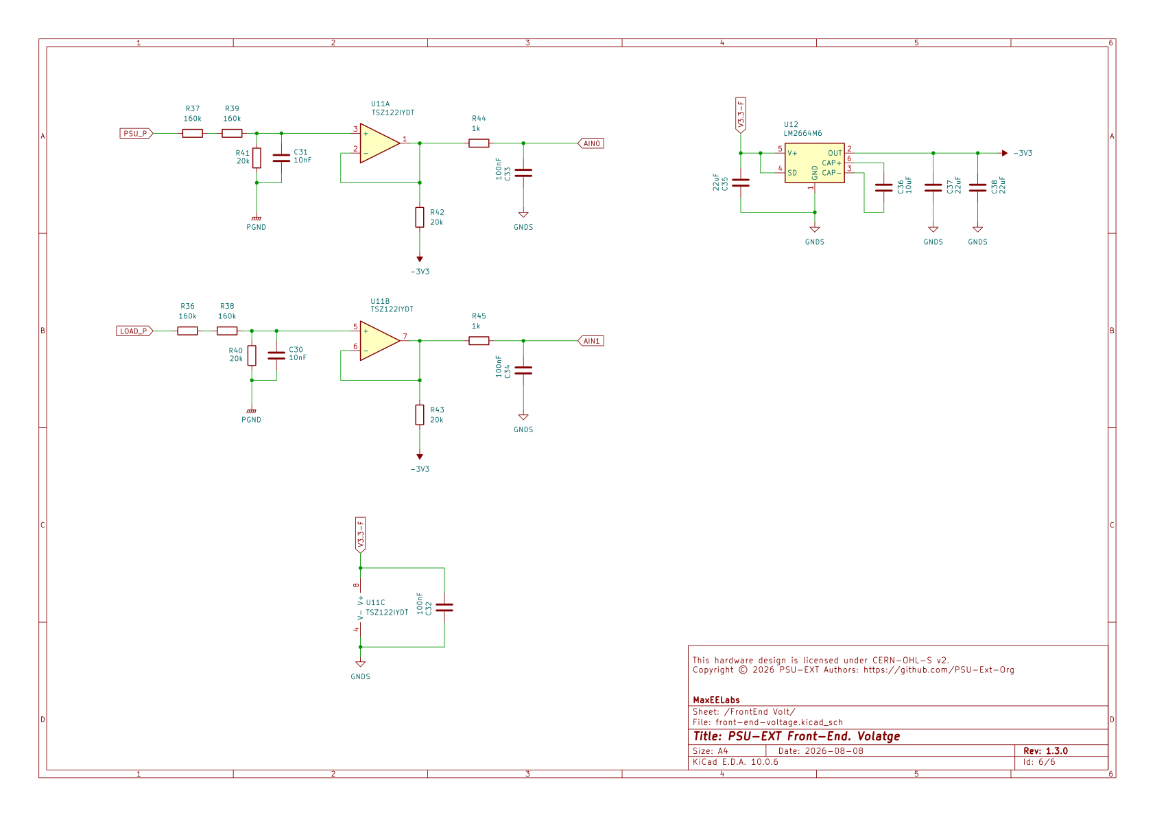
The revised design places a TSZ122 dual precision operational amplifier between the voltage dividers and the ADC. Each amplifier channel is a unity-gain follower. The divider sets the voltage ratio, and the buffer provides a low-impedance signal to the converter.
Measured voltage
      |
    160 kΩ
      |
    160 kΩ
      |
      +----> TSZ122 follower ----> 1 kΩ ----> ADS1115
      |                                      |
     20 kΩ                                 100 nF
      |                                      |
     GND                                    GND
A 10 nF capacitor also sits across each divider's 20 kΩ resistor. The buffer drives the 1 kΩ / 100 nF filter at the ADC input.
This gives the voltage channels an actively driven input, as the current channel already has. The aim is to preserve consistent voltage readings while changing the PGA range and ADC rate.
Getting the Buffer Close to Zero
The next experiment focused on the bottom of the measurement range. A voltage follower needs to follow its input down to ground. A rail-to-rail output specification still leaves a finite output swing limit that depends on loading.
In an initial MCP602 follower test, grounding the input produced about 3 mV at the output. With a 17:1 divider, that corresponds to 51 mV referred back to the measured input. For the new buffer circuit, operation close to ground deserved its own solution.
We added a resistor from each buffer output to a negative rail:
Divider ----> TSZ122 follower ----+----> ADC filter
                                 |
                               20 kΩ
                                 |
                         -3.3 V charge pump

TSZ122 supply pins: +3.3 V and GND
An LM2664 (U12 on the image below) charge pump generates the nominal -3.3 V rail. Each 20 kΩ resistor draws approximately 165 µA when the buffer output is near 0 V. This keeps the amplifier sourcing current as its output approaches ground.
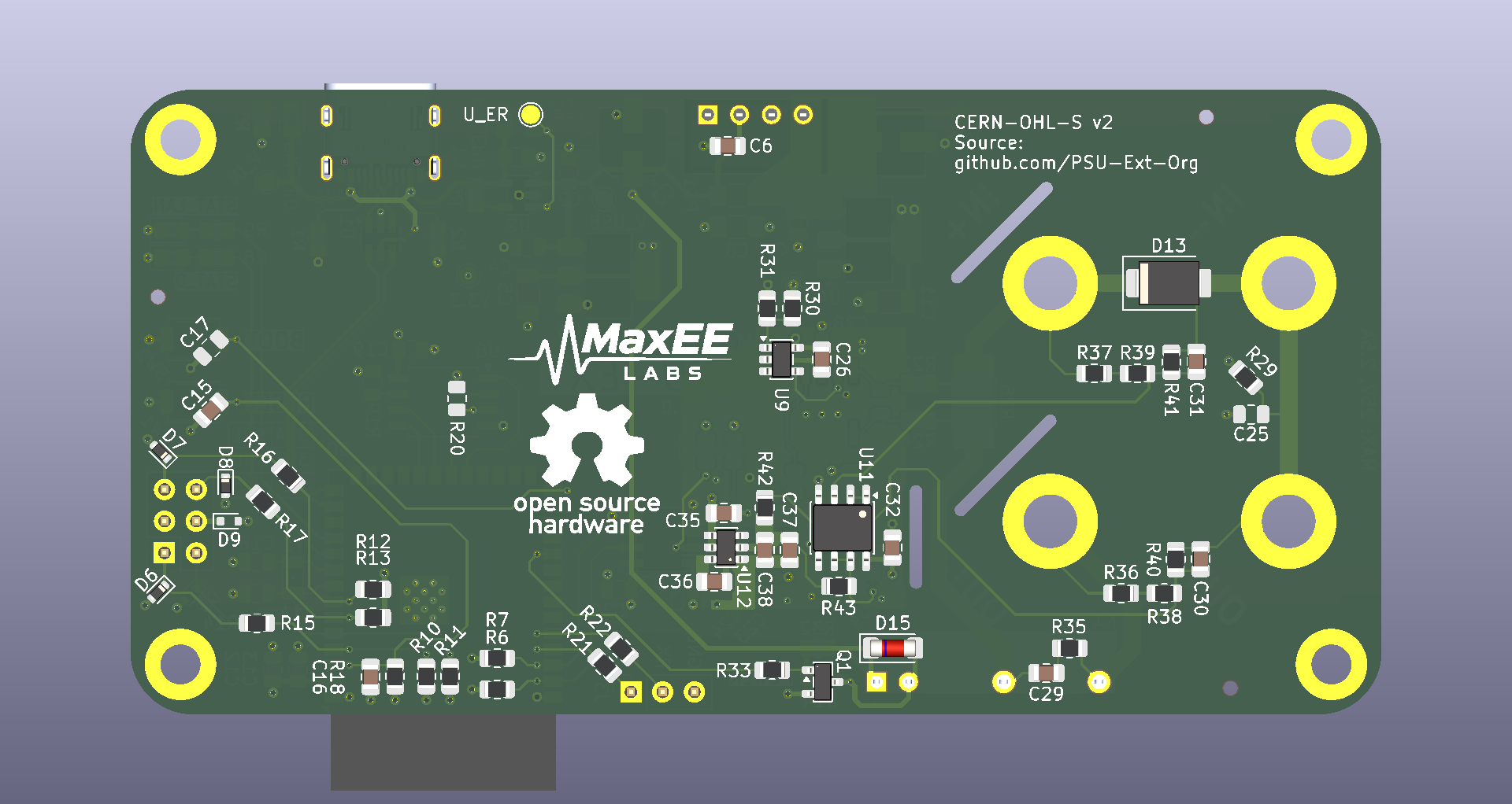
The negative rail connects through the output resistors. The TSZ122's supply pins remain at ground and +3.3 V on the isolated measurement side.
Art Kay describes this technique in Texas Instruments' Single Supply Op Amp with True Drive to GND. The pull-down provides a current path to the negative supply, allowing the amplifier's lower output transistor to turn off near ground. It is a useful way to extend a single-supply buffer's operation toward zero.
The Dual-Supply Alternative
Another approach is to power the buffer from positive and negative rails, placing ground inside its output range. That would require suitable supply voltages for the selected amplifier.
The TSZ122 operates from a total supply voltage of 1.8 V to 5.5 V same as other modern precision opamps. Directly connecting it across +3.3 V and -3.3 V would apply 6.6 V. Regulated ±2.5 V or ±1.8 V rails would fit its operating range, but generating and regulating those rails would add components and board space.
For this revision, the output pull-down arrangement lets us retain the existing 3.3 V amplifier supply and use the charge pump for output bias.
Breadboard Results and the Next Boards
Breadboard tests with the TSZ122 and MCP602, using the charge pump and output pull-downs, have shown approximately 1 mV resolution in the 0–0.2 V measurement region. That is a good result for the new front end.
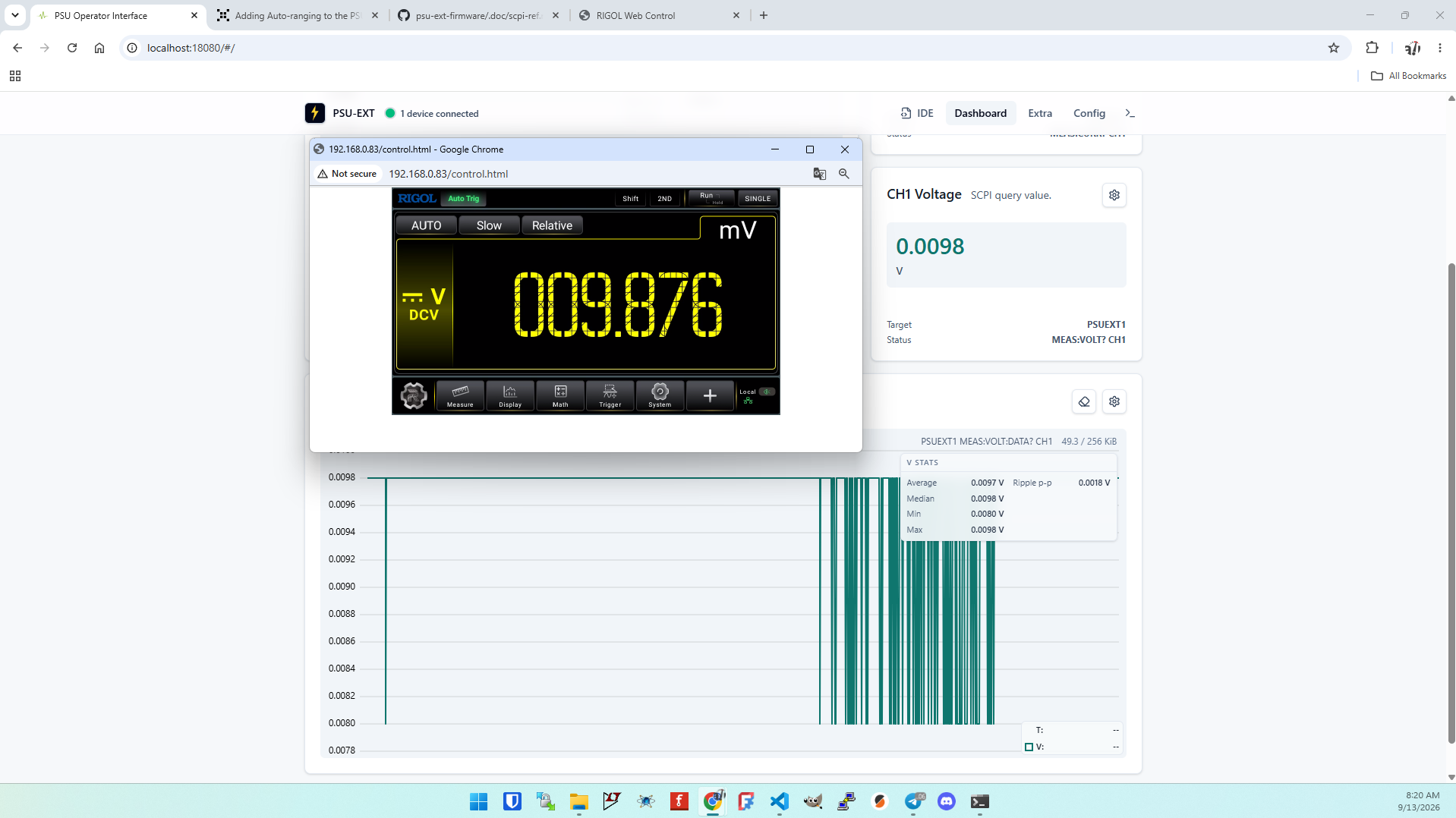
The revised boards are on order, and we are waiting for them to arrive. The new board's resolution is TBD. We will measure it on the assembled hardware, alongside voltage accuracy and behavior across the programmable ranges and rates. The breadboard result describes resolution; a new accuracy specification will come from those measurements.
The development started with a working fixed-PGA, fixed-ADC-rate design. Adding autoranging and programmable acquisition speed led us through the divider, the buffer, and the buffer's output stage near ground. The next step is to put that complete signal path through its measurements on the new boards.
If you like the article, please support us by following PSU-EXT on Crowd Supply. You'll receive more project updates and launch news.
Discussions
Become a Hackaday.io Member
Create an account to leave a comment. Already have an account? Log In.