 Aditya56h
Work date:** 8 September 2026
The three upper PCBs have now been assembled into the first practical digital stack.
The setup uses a current-limited laboratory supply, J-Link for STM32 debugging and USB access to the iCESugar Pro FPGA module. This arrangement lets us inspect each layer while keeping the Analog Board disconnected.
During bring-up we checked the important power and reset conditions. The FPGA core domain measured near 1.2 V, the I/O domain measured near 3.3 V and the PHY reset signal was active. A short involving two pins was also identified and corrected. The STM32 and FPGA communication path was exercised after the correction.
This is useful progress, but it is still board-level bring-up. A powered Ethernet connector and healthy reset level do not prove that the PHY can identify correctly, establish a cable link or transfer packets. Those checks will be retained as a separate milestone with MDIO register evidence, link status and captured traffic.
The assembled hardware is also providing the first reliable physical reference for the enclosure. The real board outline, mounting holes, connector heights and cable directions matter more than the approximate component placement in the original assembly export.

Assembled upper stack under current-limited bench power.
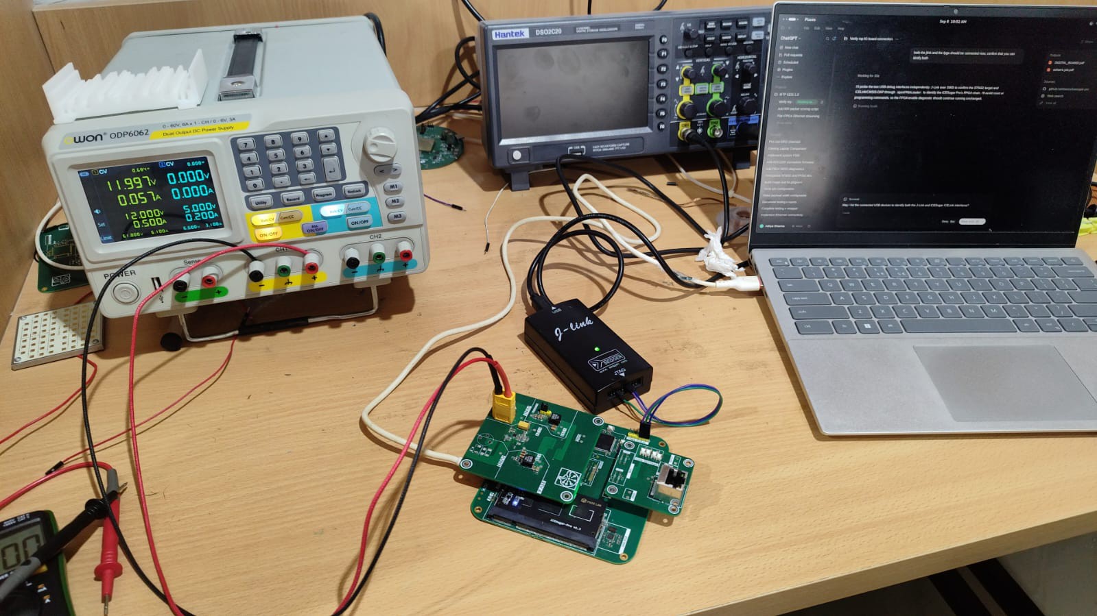

Close-up of the Top Power, Top I/O and Digital EEG assembly
Discussions
Become a Hackaday.io Member
Create an account to leave a comment. Already have an account? Log In.