 JP Gleyzes

Specification
My son wanted a high accuracy accelerometer board to characterize a vibrating pot.
Here is an accurate (but still cheap) measurement board.
Specifications are :
- 3 x 3 axis accelerometers 20bits accuracy
- +-10g acceleration range
- 3 sensors fully synchronized
- high rate of acquisition (up to 4kHz. Target 2kHz)
- interfaced with PC via USB
Critical point of this specification is the requirement for synchronization of the 3 sensors. This forbids cheap accelerometers such as MPU6050...
The selected chip was thus ADXL357. It exposes SYNC signal to trigger acquisition on several chips in parallel and can be intercaed with MPU with highspeed SPI bus.
Here are its main features :
- 0 g offset vs. temperatures (all axes): 0.75mg/°C maximum
- Ultralow noise spectral density (all axes): 75 µg/√Hz
- ADXL356 has user adjustable analog output bandwidth
- ADXL357/ADXL357B digital output features
- Digital SPI and limited I2C interfaces supported
- 20-bit ADC
- Data interpolation routine for synchronous sampling
- Programmable high- and low-pass digital filters
it also offers
- Integrated temperature sensor
- Voltage range options
- VSUPPLY with integral regulators: 2.25 V to 3.6 V
- V1P8ANA, V1P8DIG with internal LDO regulator bypassed: 1.8 V typical ± 10>#/li###
- Operating temperature range: -40°C to +125°C
Analog Device sells evaluations boards which are perfect to be integrated on the vibrating pot. We needed 50cm wires in "star configuration" from the ESP32 to the 3 sensors fixed on the pot
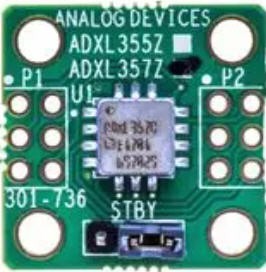
Full specification of this board is here
Note that Synchronized measurement is achievable only with EVAL-ADXL357Z board. The ADXL357 chip has a hardware SYNC pin which is exposed on this eval board.
The SPI bus allows to sustain the high rate of acquisition :
Reading one ADXL357 sample means 3 axes × 20 bits, packed in 9 data bytes, plus an address byte — call it ~10 bytes per sensor. At 2 kHz × 4 sensors, that's 80 kB/s of payload on the bus, or ~640 kbit/s plus transaction overhead (CS toggling, register addressing). The ADXL357 accepts SPI clocks up to 10 MHz; even running conservatively at 4–5 MHz for cable-robustness , each read cycle of all 4 sensors takes roughly 100–150 µs. Sample period at 2 kHz is 500 µs, so the bus is busy well under a third of the time.
ESP32-S3 MPU
USB link. The spec's frame is ~38 bytes (magic + 32-bit counter + 4×3 packed 20-bit axes + CRC16) × 2 kHz ≈ 76 kB/s — well under the spec's own 200 kB/s ceiling, and the ESP32-S3's native USB CDC sustains around 1 MB/s in practice. Order of magnitude of headroom.
CPU. The S3 runs dual-core at 240 MHz. At 2 kHz we have 500 µs per cycle; the SPI reads plus packing plus CRC take a fraction of that in C/C++. The dual core is used in standard pattern — one core handles the SYNC timer ISR and SPI reads into a ring buffer, the other drains the buffer to USB — makes losing frames genuinely hard.
Schematics
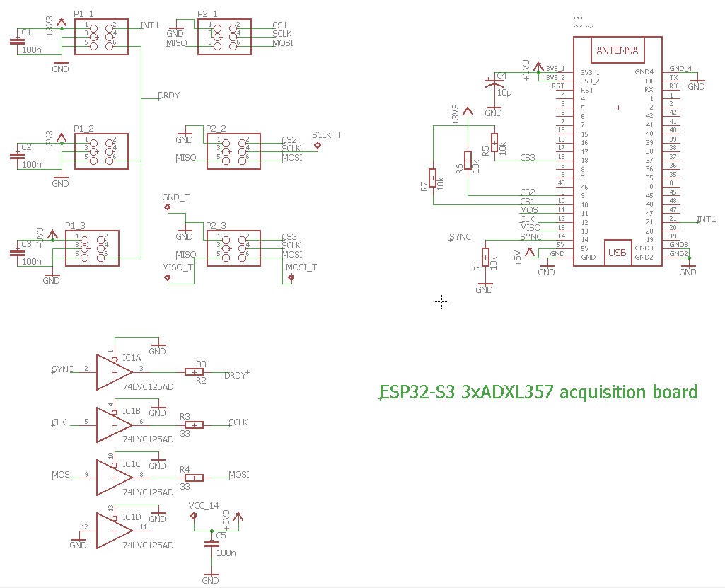
Apart from the ESP32-S3 and the connectors for the 3 ADXL537, this schematics show a buffer 74LVC125AD. This buffer (Low Voltage version) will clean up the high freqency signals DRDY, SCLK, MOSI produced by the ESP32-S3 and routed to the sensors via shielded wires.
PCB
The PCB was designed with Eagle software.
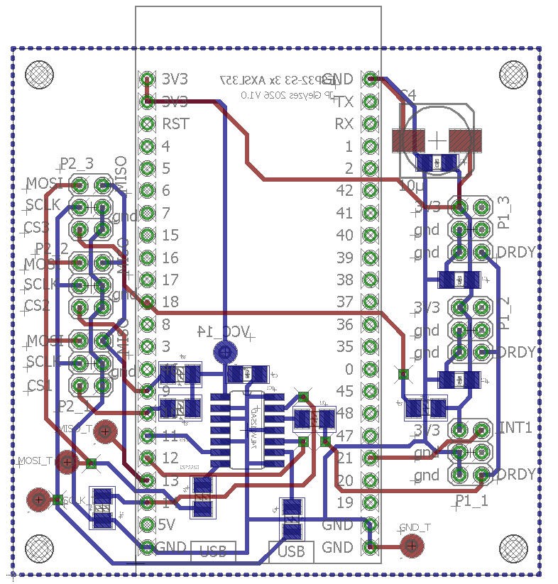
The ESP32 goes on the top side, while all the other components go to the bottom side.
PCB can be bought at PCBWay directly from this project page
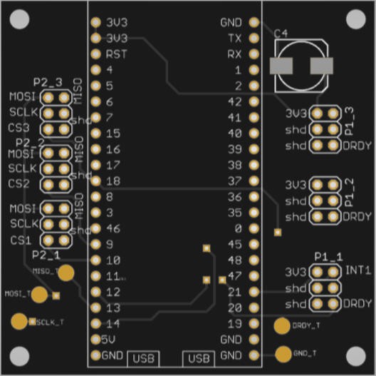
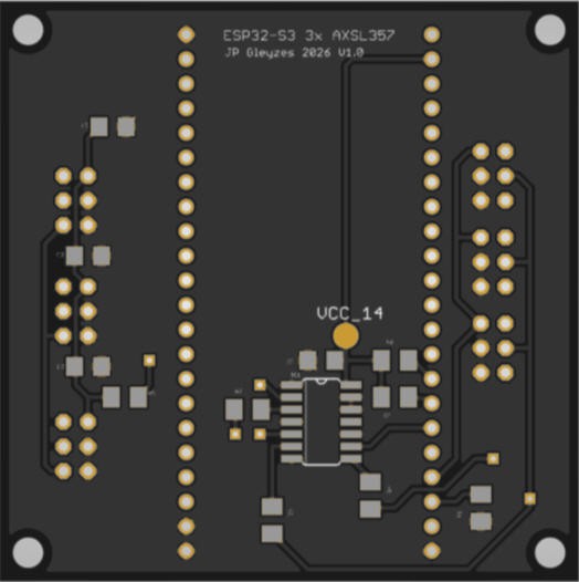
The PCB was kindly sponsored by PCBWay and is as usual of excellent quality.

and if you are new to PCBWay please use this affiliated link : https://pcbway.com/g/o35z4O
soldering is easy but special care is needed for shielded cables.
Use single core shielded cable for MOSI, MISO, SCLK, CS and DRDY. The core is soldered of the Eval board and on the ESP32 side.
the shield is only soldered on the ESP32 side (pins labeled shd)
note also that connectors P1 on eval board side must be shorted between...
Read more »
 yancan
 Maik
Maik
 Abraham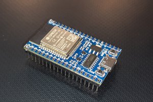
 ElectroBoy