 Jorj Bauer
Obviously, I'm prepping the r2 board. Here's where I am so far; still a few bits to clean up...
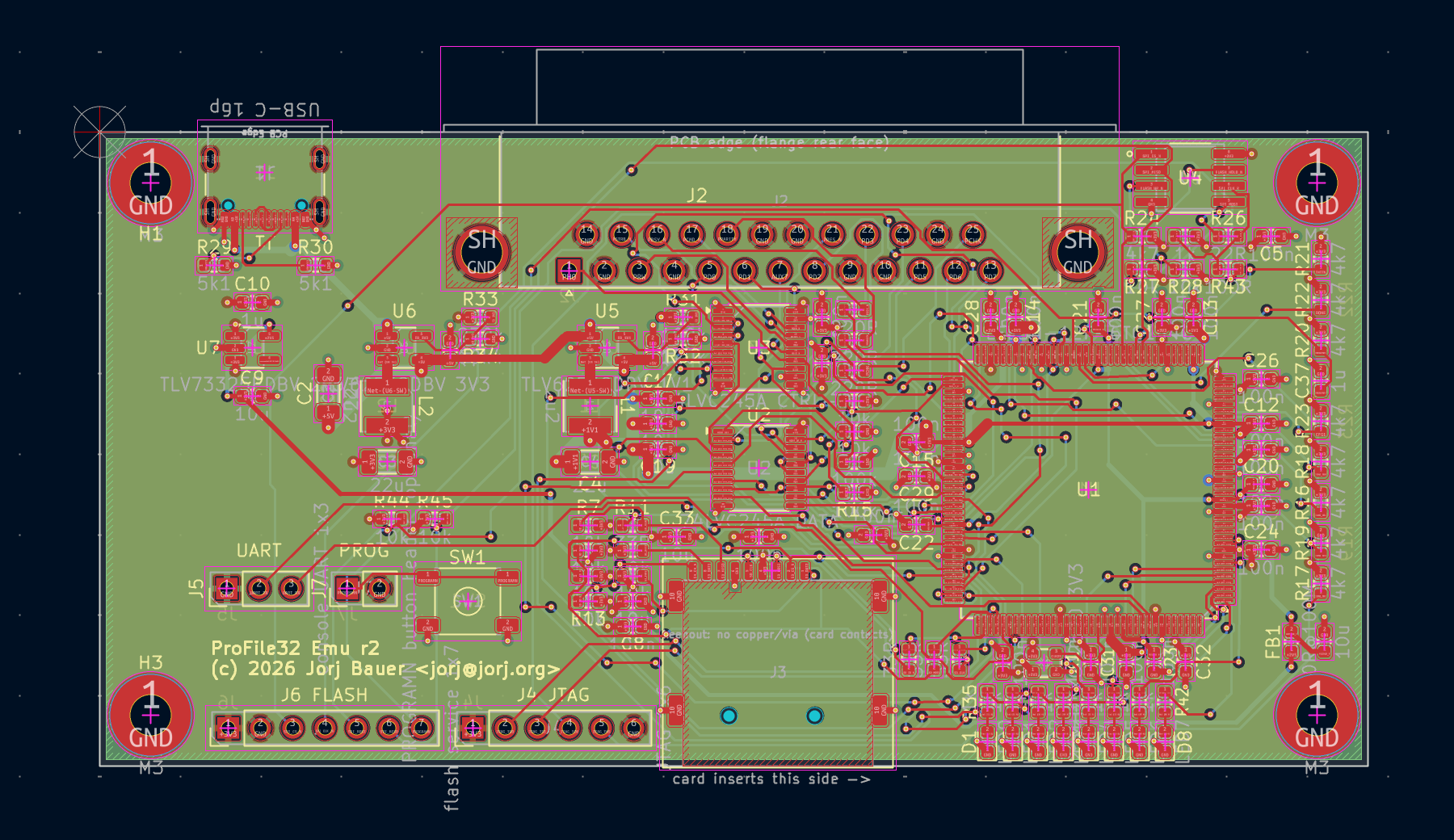
The r1 board was large and spaced out intentionally; more room to repair errors. Now it's time to crunch it down.
And while I'm smallifying the board... I'm biggifying the parts. I'd never worked with 0402 size parts before and, while I did manage to get it all working, it was not exactly fun. So we're back to 0603 here; unless I have need to shrink down more, I see no reason to use the little beasties I can barely see, and easily fling around the room accidentally. (The R3 lesson from my r1 board is really what made my mind up here: I dropped a 220 ohm resistor, picked up another resistor that was right there that I thought was the one I dropped, but it was a 10k.)
I've also dropped the parts I never used - the USB-C JTAG driver and all its support electronics are gone. I left in the LEDs because LEDs are cool, but they can be left out in a final build. As can the flash and jtag headers. I'll just need some way to initially program the flash (maybe an SOIC adapter, program them before they're even on the board).
The buck regulator pinouts are corrected; I've changed the footprint for SW1 to match what I've got sitting around; added a few passives to correct missing pull-ups that should make the flash more reliable, and stub terminators where the leads continue to an unpopulated header.
One thing I have to give up here, though: I really like having all the part labels right next to the parts. I've packed a lot of parts in places where I can't necessarily do that... so they're all on the back.
I also want to address a minor noise issue here. I've always been able to hear high frequency noise - like flyback transformers in CRTs. I've lost some of my hearing but that's never faded. Consequently, I was not surprised to hear the buck circuits doing their thing. For those that don't know how they work: high efficiency voltage converters work by rapidly turning on and off the supply, storing energy in magnetic fields and converting it back to electrical supply in a carefully timed dance. The frequency at which it switches on and off is usually very high, so that we can't hear what it's doing - something in the MHz range, well above what any animal can hear. But some parts (and, notably, the parts I picked for r1) do their best to be ultra-efficient; if the demand for current is not high, then it falls back to a much slower speed to save power. In this case, the TLV62568DBVR normally runs at 1.5 MHz and absolutely drops to something I'd estimate at 16kHz. Which is undocumented (the frequency, that is; the behavior is well documented as a power saving measure). There's no way to tell it to not do that, and it is very annoying. So we'll switch to the TPS62A01APDDCR - this is a forced-PWM-mode device that does waste a few extra mA of power, but should stay at its 2.4MHz switching speed so that we don't hear it. (Okay, so that *I* don't hear it.) The cost? Well, I've got a few of the old parts that will now do nothing. Some new inductors and resistors. And overall? It's actually cheaper, by about $1.34/board.
In a couple weeks, we'll see how the r2 PCB fares. And in the mean time, at least I've replaced the pile of boards and adapters with a single bodged-together PCB!
Discussions
Become a Hackaday.io Member
Create an account to leave a comment. Already have an account? Log In.