 Justin Davis


Project goals:
- Retrocomputer using 1970s/early 1980s type of technology
- Through-hole only (strongly preferring DIP)
- Only parts in active production (no ebay/shady distributors)
- An instruction set that is fun to program
- No racing the beam
- No counting instructions for timing
- Bare-metal - no virtual machines to program
- Therefore, a true von Neumann CPU (no Harvard)
- Native storage so you can write and save programs on the machine itself
- Fast as the day is long
Why PLDs?
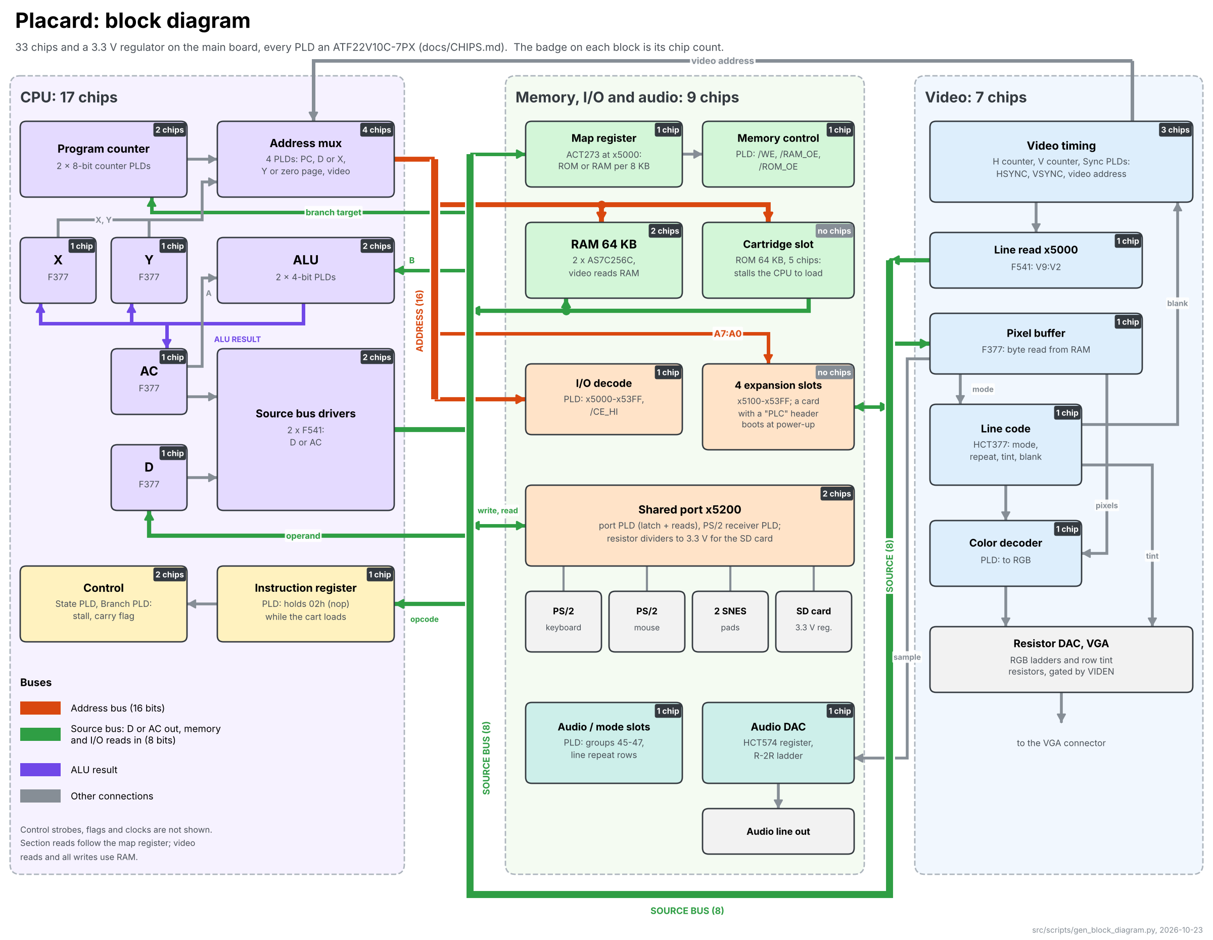
The project started as a pure 7400-series computer, but to meet the goals I conceded it would take too many simple gate chips to achieve it. So I swapped some gates for 22V10s. The first PLA was on the market in 1970 - the first PLD in 1977, so thematically it still meets project goals. It ended up 33 chips on the main board plus a 3.3 V regulator, and 3 on the cartridge.
This computer was inspired by the ones which came before - the Gigatron, Ben Eater's, Novasaur, Isetta. There are similarities in the architecture.
CPU
- 8-bit data, 16-bit address, von Neumann, 25.175 MHz clock (the VGA pixel clock).
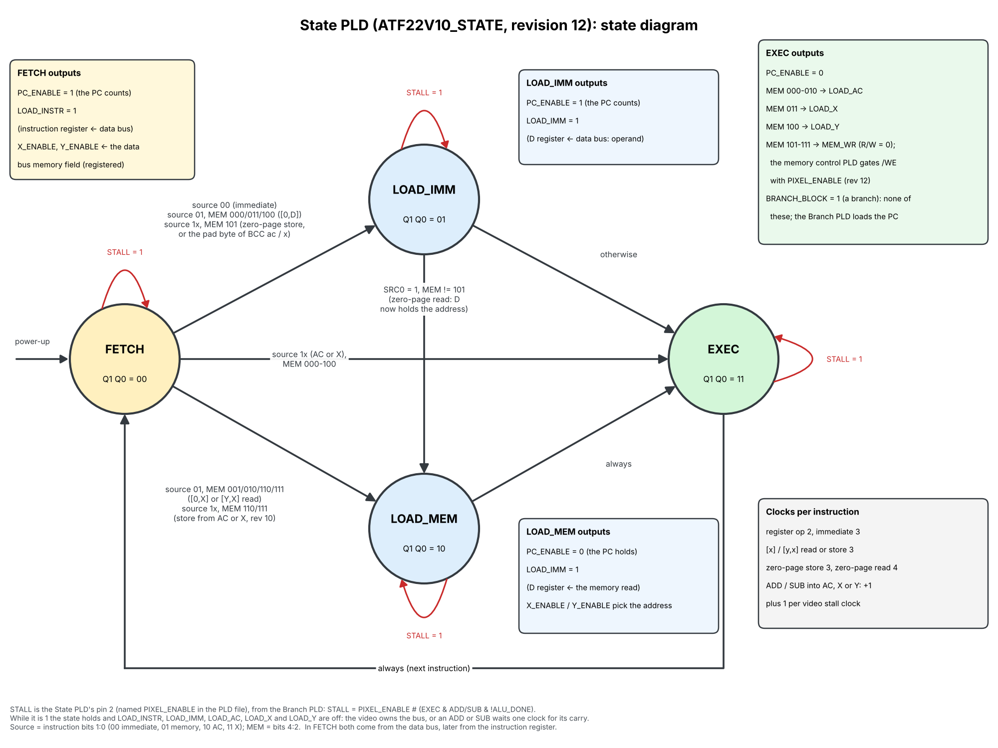
- Instructions take 2, 3 or 4 clocks
- Registers: accumulator, X, Y and D (immediate/memory operand), each a 74F377.
- Controlled by a 4-state machine (FETCH, LOAD_IMM, LOAD_MEM, EXECUTE) in one PLD
- ALU: two 22V10s, 4 bits each, with zero, sign and a carry flag (reminiscent of the obsolete -181 ALUs)
- Program counter: two 8-bit loadable counter PLDs.
- Address mux: four PLDs pick Program Counter, zero page, [Y,X] or the video address.
- Addressing: immediate, [0,D] and [0,X] zero page, and [Y,X] 16-bit.
- Instruction register is itself a PLD, which also holds a NOP while the cartridge loads so the CPU waits without gating the clock.
Video
- 640x480 VGA at 60 Hz, generated by H counter, V counter and sync PLDs.
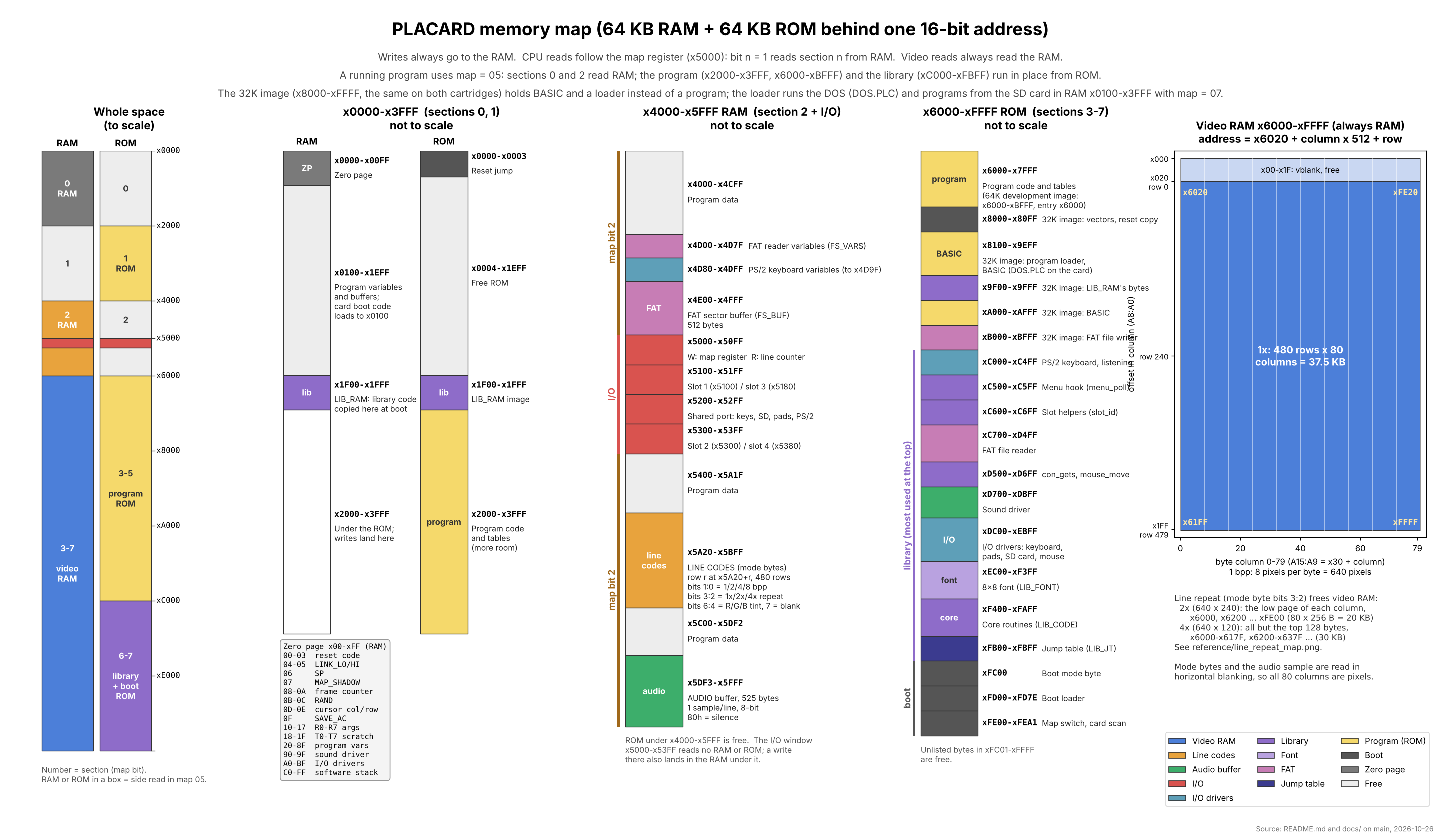
- Uses RAM as raster memory (x6020-xFFFF)
- Video runs automatically - stalls CPU when it needs to read from RAM
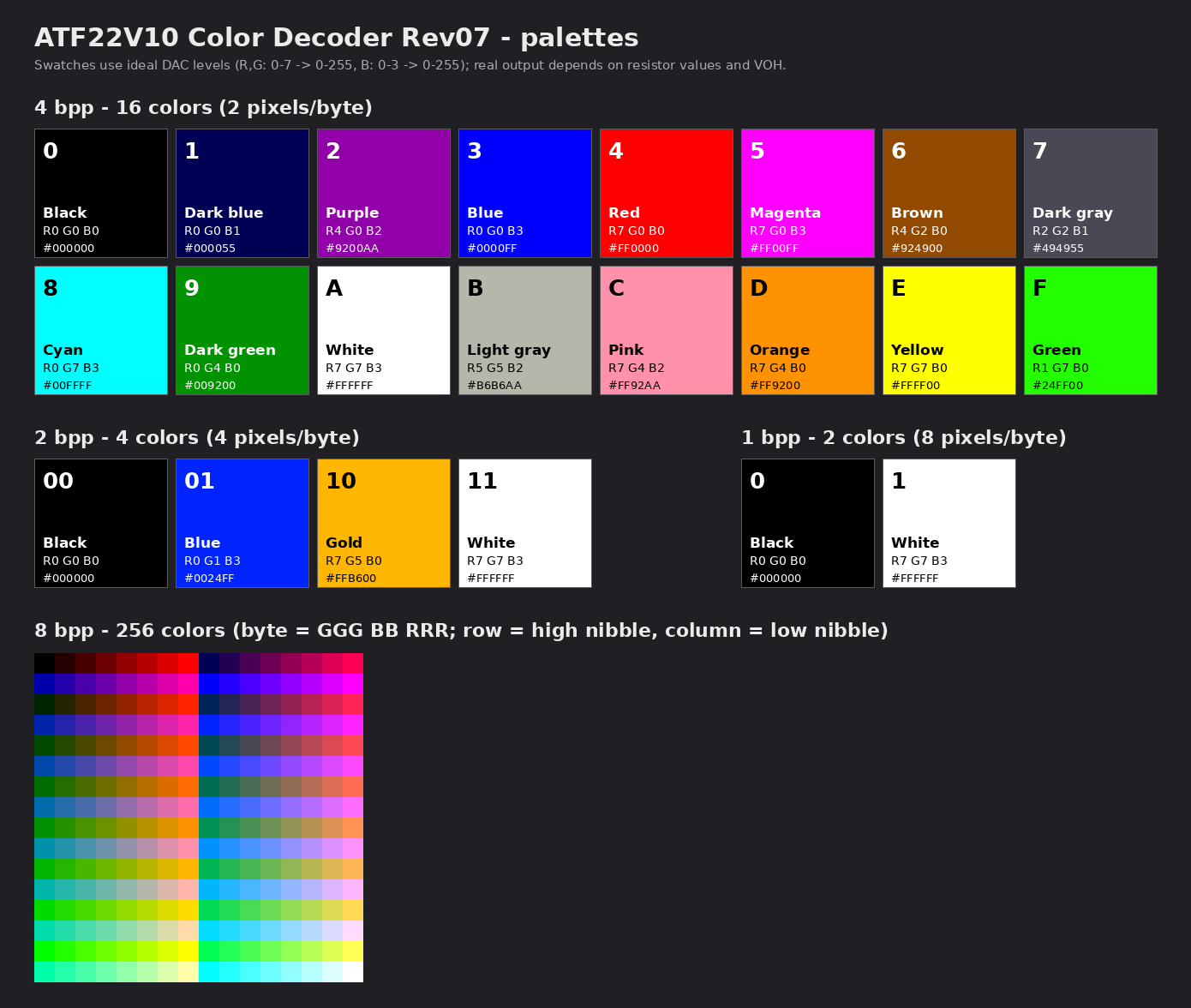
- Colors modes are adjustable per line:
- 640 monochrome pixels or
- 320 4-color pixels or
- 160 16-color pixels or
- 80 256-color pixels
- RAM can be conserved by select lines to repeat
- 1x mode reads every line
- 2x mode skips every other line (half of required RAM)
- 4x mode skips 3 lines at a time (quarter of required RAM)
- Modes mix freely down the screen: 80-column text above a 256-color picture, for example.
- Each row can be tinted with another 8 colors
- Gives colored text backgrounds and raster bars for free.
- Provide some background color in monochrome mode
- Provide color gradients in other color modes
- Each RAM byte is processed by the Color Decoder PLD which turns it into RGB with a resistor DAC.
Memory
- 64 KB RAM (two AS7C256 15 ns SRAMs) and 64 KB of ROM space behind the same addresses, in eight 8 KB sections;
- A 8-bank select register picks RAM or ROM per bank for reads (writes always go to RAM)
- Dedicated I/O window at x5000-x53FF address space
- The video reads the same RAM as the CPU: the video area is x6020-xFFFF, and the video circuit steals clock slots from the CPU in a fixed pattern, so software never has to time its code to the beam.
Sound
- Borrows video automation counter to read one 8-bit sample per scan line (31.47 kHz, one frame),
- Load your sound table and sit back. No worrying about getting the next sample ready in time.
- Latched into a 74HCT574 and an R-2R ladder DAC to a line-out jack.
- Library ROM makes tones, notes, noise and sample playback.
I/O
- PS/2 keyboard and PS/2 mouse (a PLD shifts in each byte).
- Two SNES game pads.
- SD card (SPI, FAT16/FAT32, read and write).
- Four expansion slots with their own boot code hook (like the Apple II).
- Cartridge slot: the cartridge holds the ROM image in a (slow) EEPROM
- Copies it into fast SRAM at power-up while it stalls the CPU.
- 32K and 64K cartridge boards are designed.
Software
- Standard library in ROM with an append-only jump table: 16-bit math, multiply/divide, text console with line input, graphics, keyboard, mouse, pad and SD drivers, a FAT file reader/writer,...