Marcel van Kervinck
-
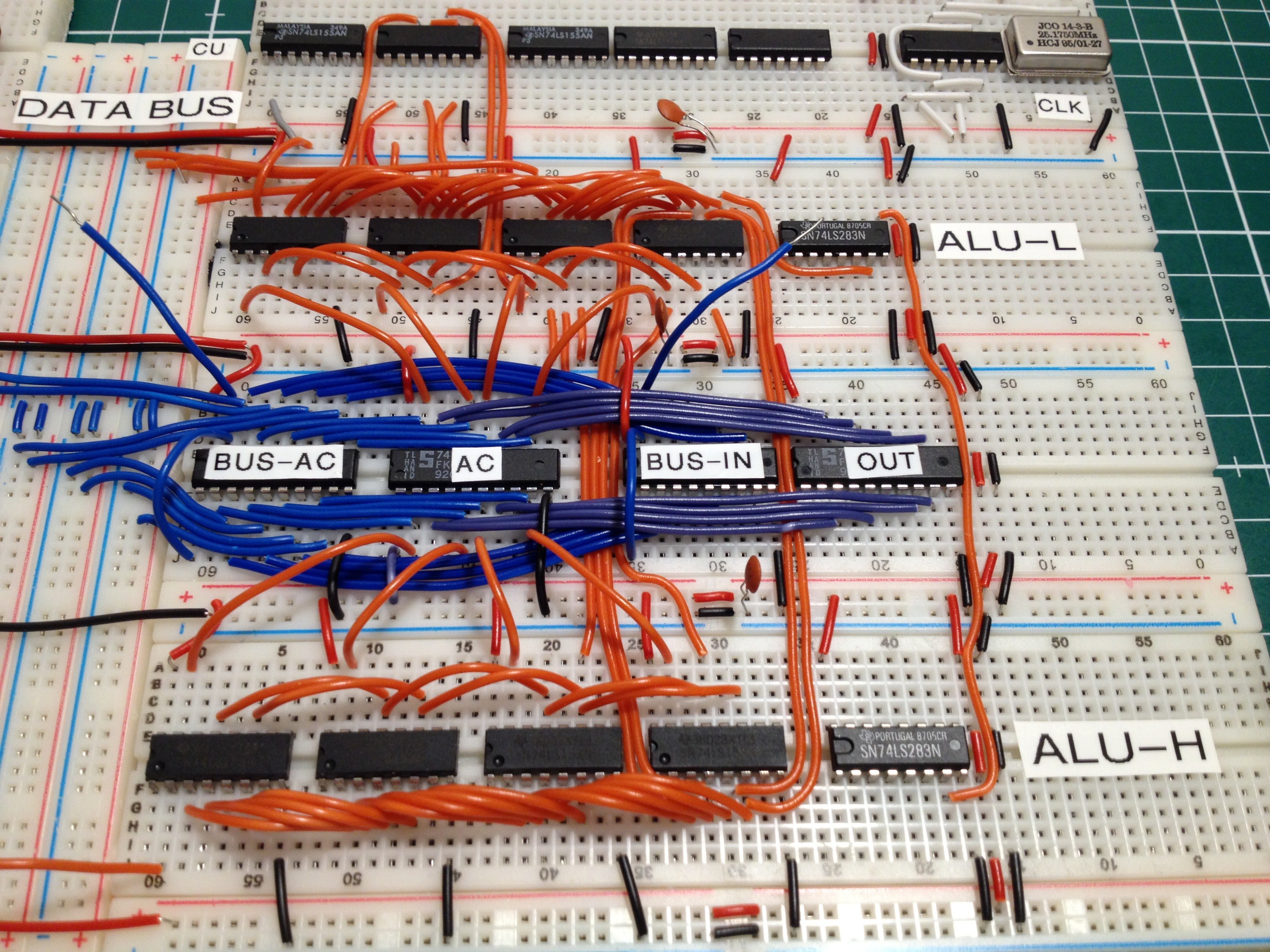
ALU almost wired
04/08/2017 at 20:08 • 0 comments![]()
I just hope I didn't misread any data sheet
-
Guess which ALU concept I'll go with
04/07/2017 at 14:19 • 0 commentsFirst some perspective:
![]()
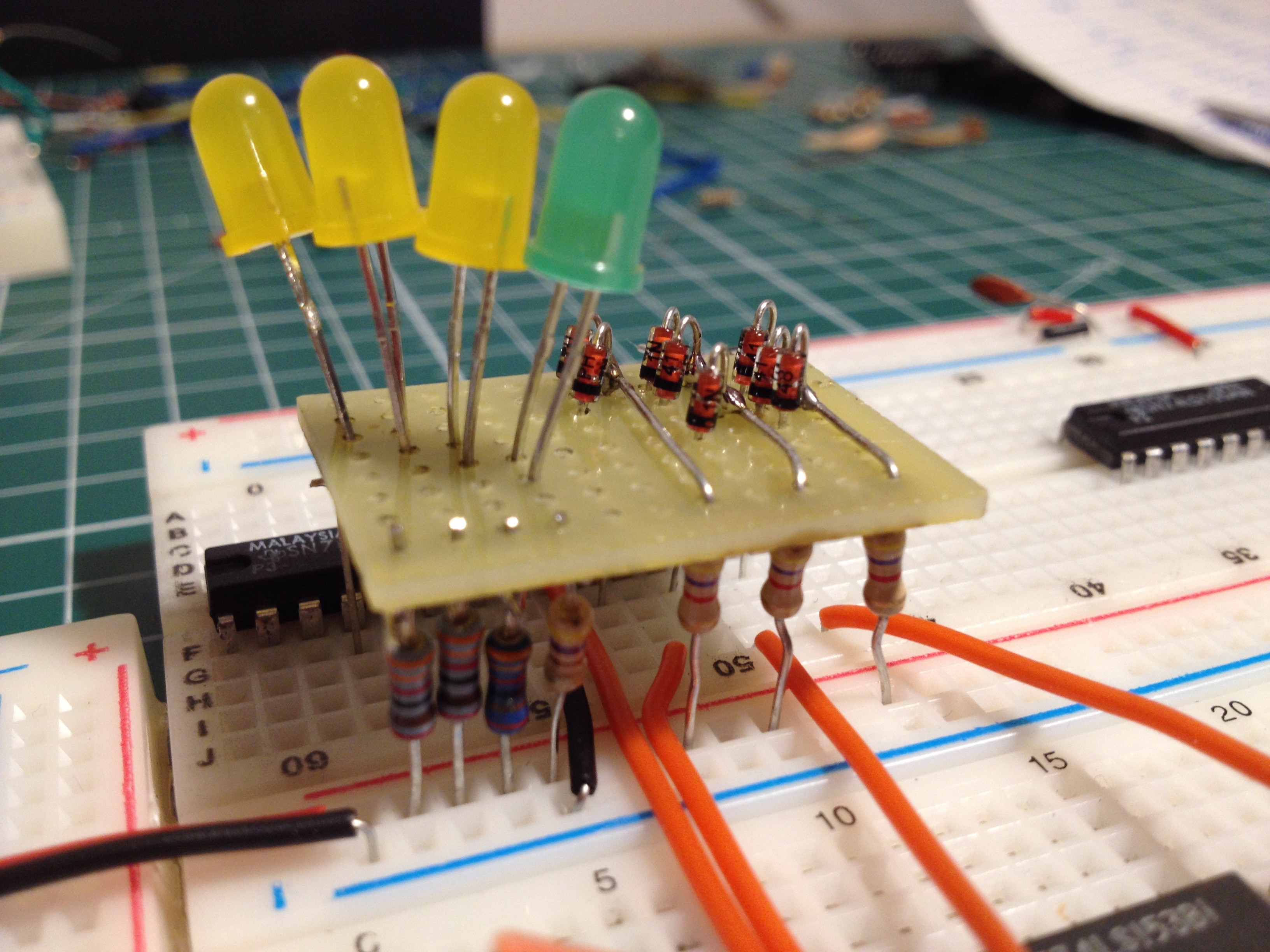
Yes, the ALU will be made out of multiplexers! (74LS153)
![]()
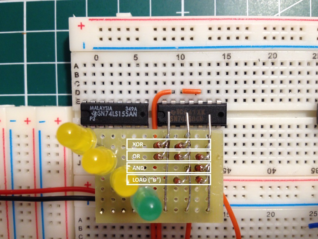
The 74LS155 that is to become a 3-to-8 opcode decoder, the bottom half of the diode ROM matrix and the inverter/buffer row (74LS04). You can see XOR, OR, AND and LOAD programmed here.
![]()
-
Testing a bunch of diodes
04/05/2017 at 19:58 • 0 commentsI'm still uneasy about the planned ALU layout and its control logic. The way to extract "write" and "jump" signals remains clumsy and the STIX instruction doesn't really fit in well yet. It will work, but that one remains a wart. Besides, the alternative ALU, the 10 chip MUX-based design, remains much more attractive.
So I revisited it and realised that of the 8 control lines only 5 matter. That's good news. If that can be reduced to 4 or 3 bits we're done. 4 is easy, but then we still don't have "jump" and "write" signals.
![]()
Staring at the dense part of the truth table I realised this is a ROM's job. That can decode 3 instruction bits into to 6 ALU combinations (ADD, SUB, AND, OR, XOR and "B" aka "LOAD"). Doing this in a little ROM we immediately get the "write" and "jump" for free by assigning these to the unused ALU codes. Plus, we'll have a full bit to spare in the instruction word. That might be useful for STIX. Also, managing the two clock phases can become simpler. All combined this has the potential to save up to 3 chips and that is worth exploring.
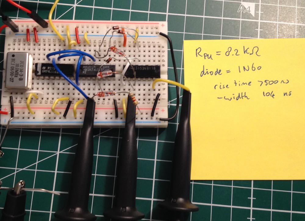
But ROM is slow. So an old idea popped up: maybe, just maybe, we can do the ALU control with a 3-to-8 decoder and a tiny, 6 word by 5 bit, diode ROM matrix? People have controlled Atari's with such contraptions and this will be much smaller. Just 20 or so small diodes. So today I got some 1N60 and 1N4148 signal diodes and started playing. I did some quick multimeter tests first: at 10 mA the 1N4148 drops 400 mV and the 1N60 is about ten times better. But both should be ok because TTL allows for a 0.4V drop. Are they also fast enough? Lets measure:
From left to right we have one 74LS161 to count, one 74LS155 to decode and the breadboard provides word and bit lines (all vertical). Both types of diodes are in between these and there is a final 74LS153 to simulate the ALU's first stage. More on that later. I put the 1N4148's on one bit line and the 1N60's on the other so I can easily compare their characteristics. In the photo I'm probing the latter. After I realised I had forgotten a pull-up resistor, the signals generally looked good if you tweak the resistor value a bit.![]()
![]()
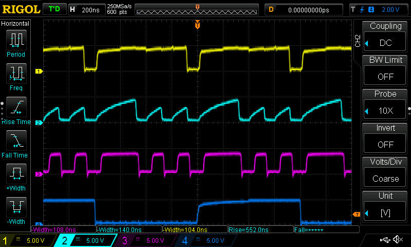
Ignore the yellow and blue. The cyan signal is the diode stage output. This signal looks poor: it has very slow rises. But once above 2V TTL has a "H", and that happens fast enough. We see the next stage (purple) rectifying it nicely. For the ALU this will be more than good enough: both diode types seem to give proper signal transfer through the ROM matrix.
So are we good? Not yet... In reality this ALU will have 8 parallel MUX chips and each one has 8 inputs. Ultimately they are all connected to the same word line coming out of the decoder.
![]()
That still doesn't sound good at all! We have an effective fanout of 8*6, + 1 for the carry. 49 is definitely more than 10. Worse, we have some nasty voltage dropping diodes in the path. Maybe this idea was too good to be true and this is a dead end. To be continued...
[ Postscript: An obvious solution to the fan-out issue is to feed the diode ROM into an inverter row. It is not really the decoder's problem anyway, as the root cause lies with the MUX-based ALU concept. We'll need 6 inverters, not 5, because one of the signals goes to 2 pins of every MUX (there are eight of them). A simple 74LS04 hex inverter IC will do the trick. An added benefit is that the ROM logic now flips from negative to positive. We can really see every operation's truth table right in front of us! And save on a few diodes along the way... ]
-
ALU design
04/03/2017 at 23:20 • 4 comments[ Edit: I eventually settled for a totally different ALU design than sketched here! Ik keep this log entry just to preserve history. -MvK ]
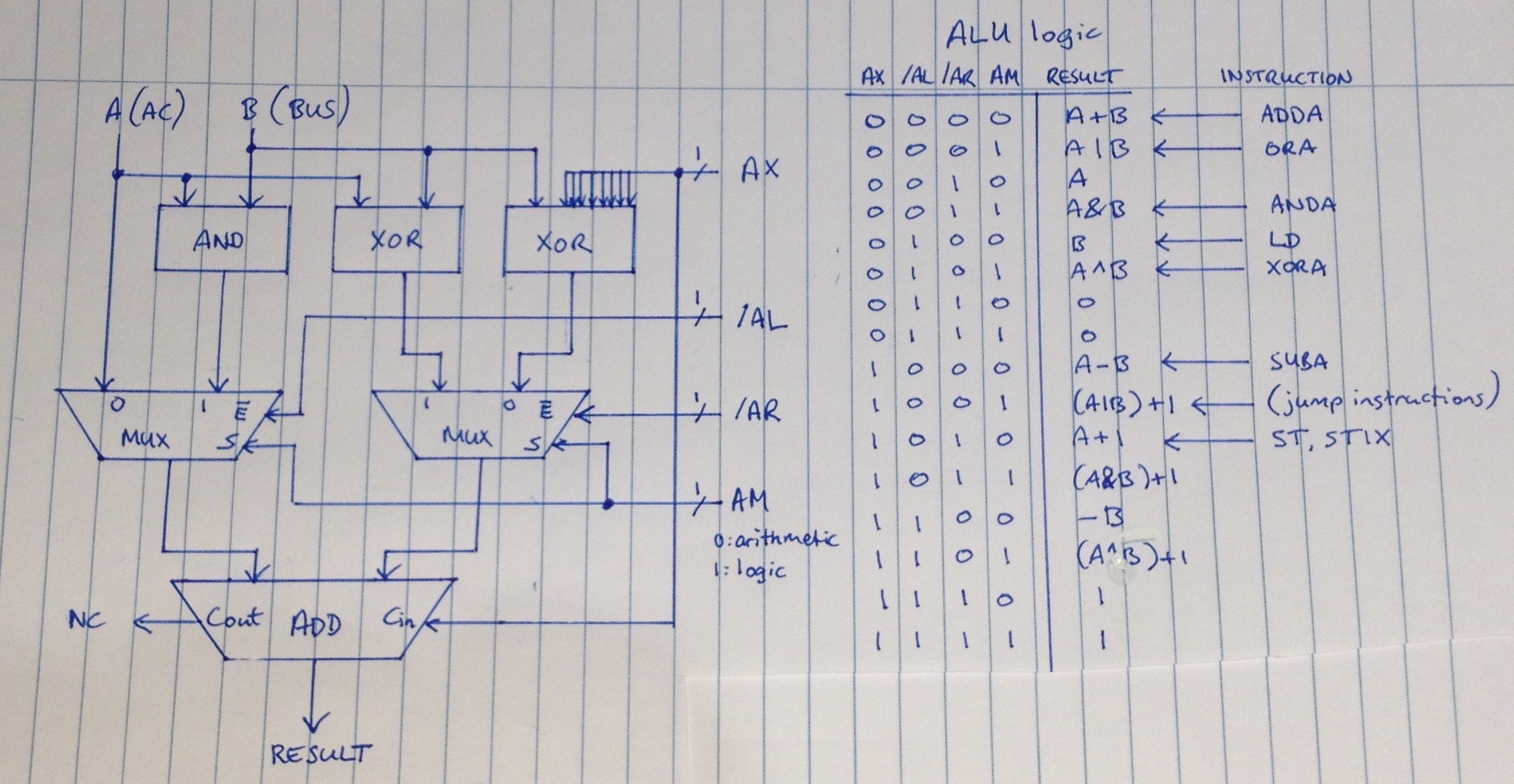
We will do a custom ALU, not because we don't have any 74'181 IC's available, but because it is more fun.
There is a beautiful 12 chip MUX-based design out there, nicely described by Dieter Mueller. It even has a shift-right instruction which the 74181 is lacking. Without that it would be 10 chips. I'm tempted to use this design but I still worry about the many control lines that go in, 9 if I count correctly. Well, 8 if we drop de SHR support. Many control lines means many chips in the decoder, unless we use a ROM but that is slow.
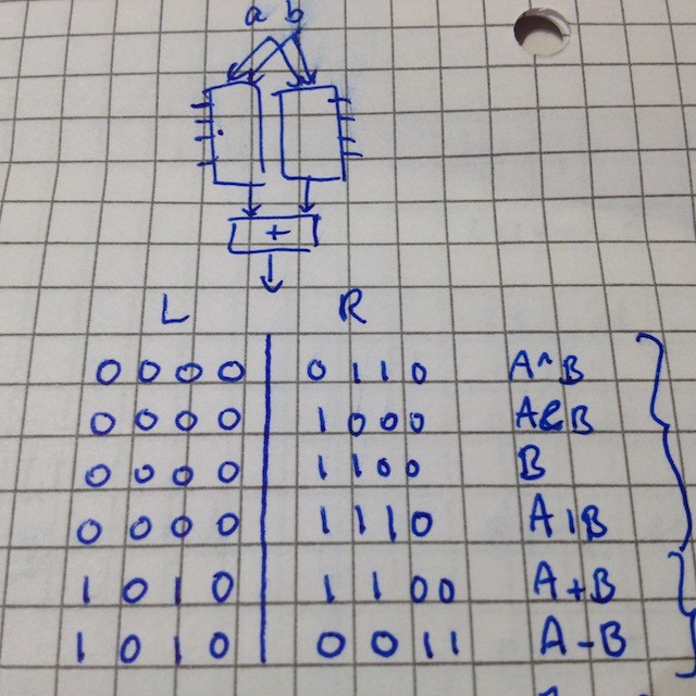
That's why I consider something else, based on 6 chips per nibble, with less flexibility but therefore also fewer control lines. The necessary operations are there (A+B, A-B, A&B, A|B, A^B). There is also a "B" operation that we can use to load data without modifying it. We need that because all traffic to registers goes through the ALU in our design. In our data path we can also put AC on the BUS, so we have things like A+A. And there is an "A+1" that we will make use of in the STIX instruction ("store-and-increment-X") later on.
The main part is straightforward: three stages, some logic on top, some multiplexers in the middle to select intermediates and a final addition stage. With 4 control lines we can generate our desired functions plus a handful more that are not very useful, such as "(A ^ B) + 1". Of our functions, only "A|B" is a bit difficult to visualise, because there is no OR-chip in the circuit. It uses the identity A|B = (A&B)+(A^B) instead. Finally, we won't store the carry as we don't want to have a status register. Maybe in a later phase we can use the carry in some useful way.
![]()
Four control lines is OK already. With that we could make an opcode scheme where 4 bits select the desired ALU operation immediately, without any further decoding, and let the other bits select the addressing modes. Then we assign the less useful codes to instructions that don't use the ALU, such as store and jump instructions. We need to derive the "write" and "jump" detectors with some logic but that shouldn't be hard. Also, during the first phase of the clock the "load" lines into the registers and the "write" line into the RAM must be muted anyway (for different reasons), which means there should be no worry for glitches while deriving these signals with combinatorial logic.
Still haven't decided yet on this one.
-
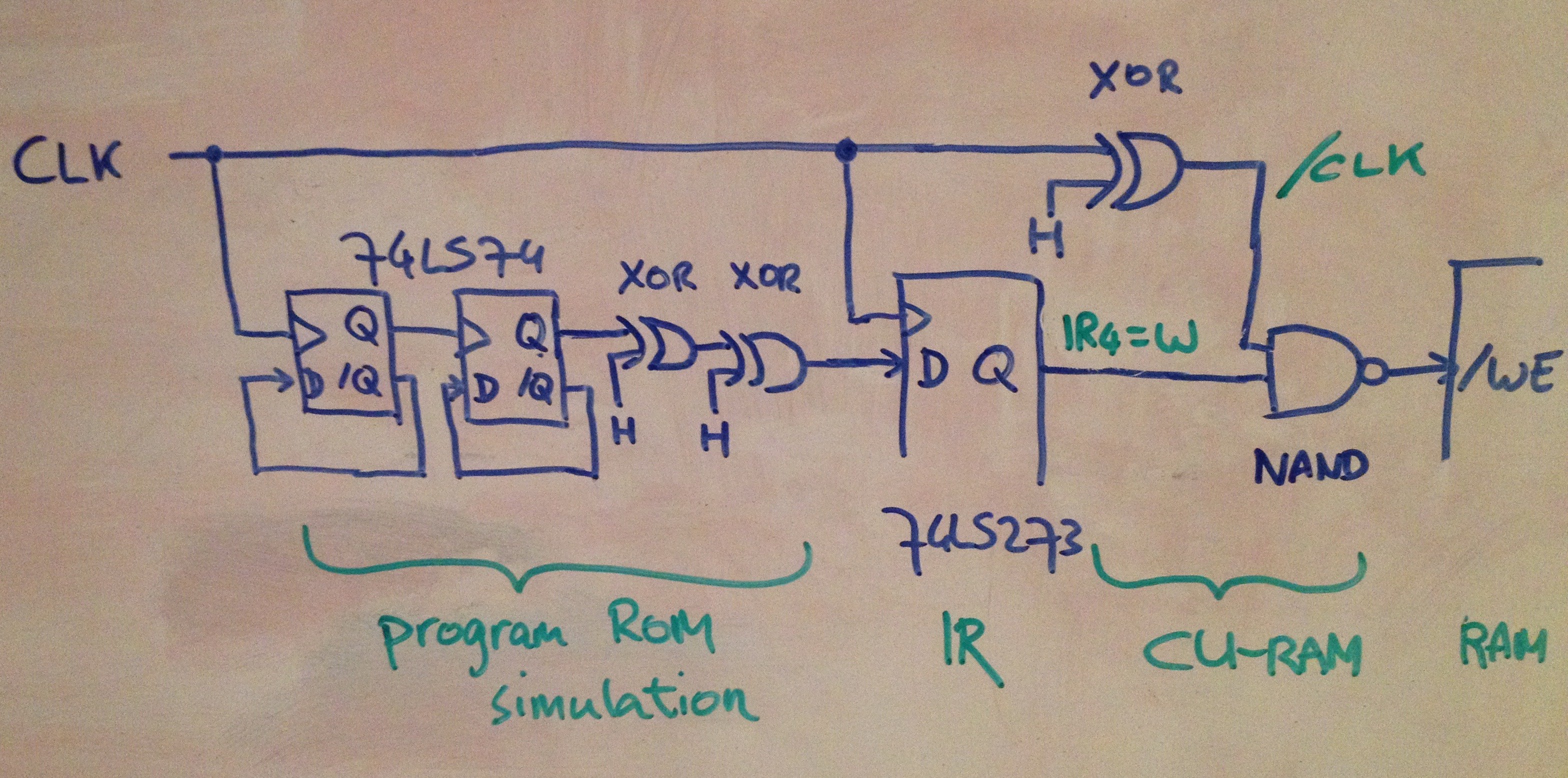
Testing the RAM write control logic
04/02/2017 at 19:14 • 0 commentsThe control unit (CU) is the last thing to be worked out before committing to a build. The concept I had in mind requires 6 chips and I was slightly unhappy about that. After some thinking I came up with an idea that drops one chip from this unit. However, it requires that at some point I invert the clock signal using an XOR gate, whereas in my original plan this would be done with a NAND. Inverting the clock with a NAND worked fine in my previous VGA project. But the XOR is slightly slower, especially if used as an inverter, so it increases the phase shift a bit further. This inversion is on the critical path towards the RAM write-enable pin. A write into RAM is only allowed to happen in the second phase of the clock. In the first phase we have to stabilise the RAM address. We don't want any glitches there so we must be really sure this is going to fly.
That's why I built a small CU-RAM simulator and fed it fake instructions: read, read, write, write, read, read, write, write, etc.. so all possible execution orders are exercised. Then just measure what the resulting write-enable signal looks like. Here is the idea in a drawing:
![]()
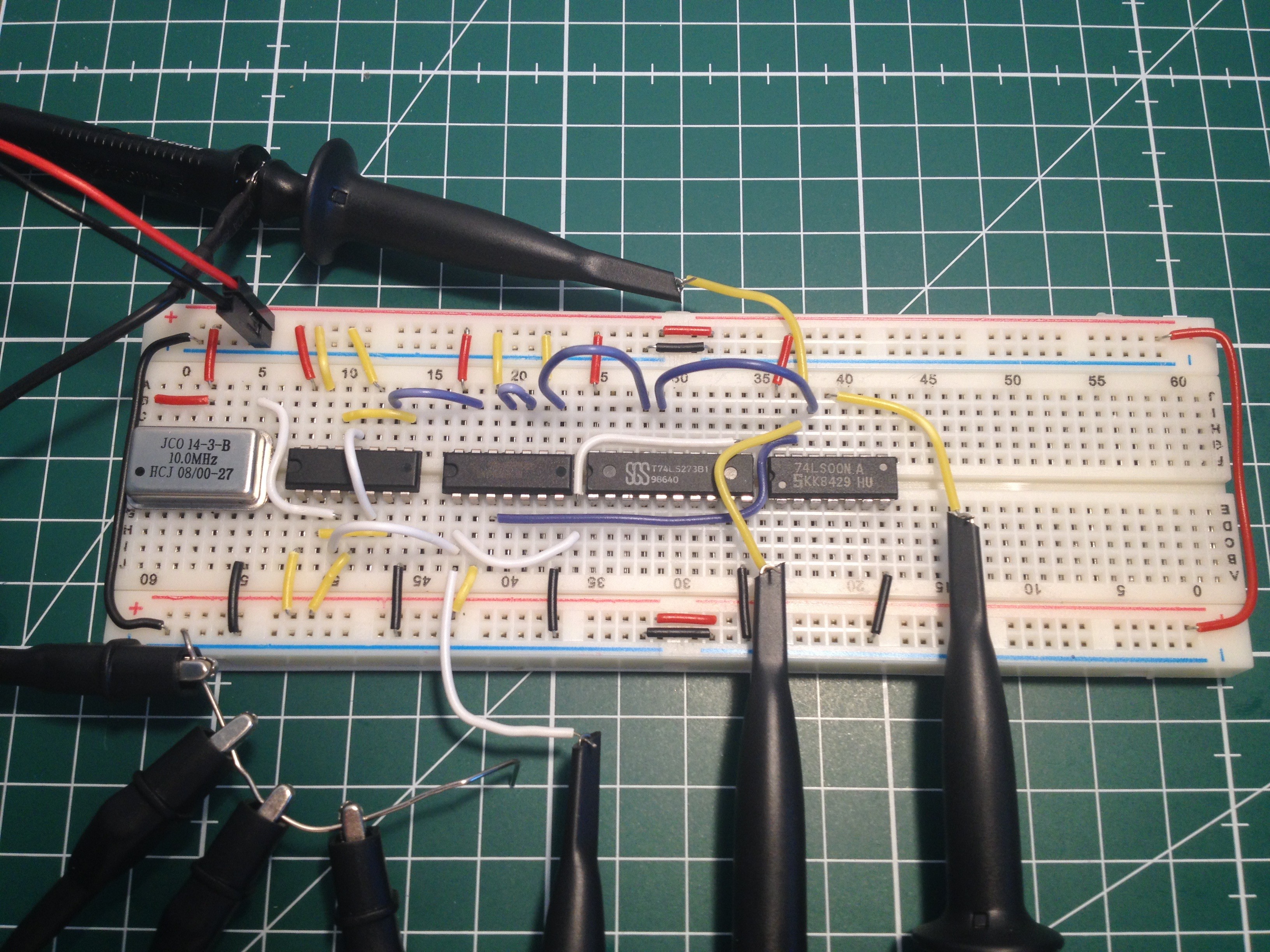
The fake instructions come from a 74LS74 dual-flipflop that just divides the clock by 4. This feeds into a 74LS273 that acts as IR register. (For fun, before entering IR, the signal goes through 2 bonus XOR inversions and picks up some delay there. This is not important but the gates were there anyway...) From the IR register it goes to the "real" NAND that on the other pin receives the XOR-inverted clock, just as in my intended design. Here the circuit on a breadboard:
![]()
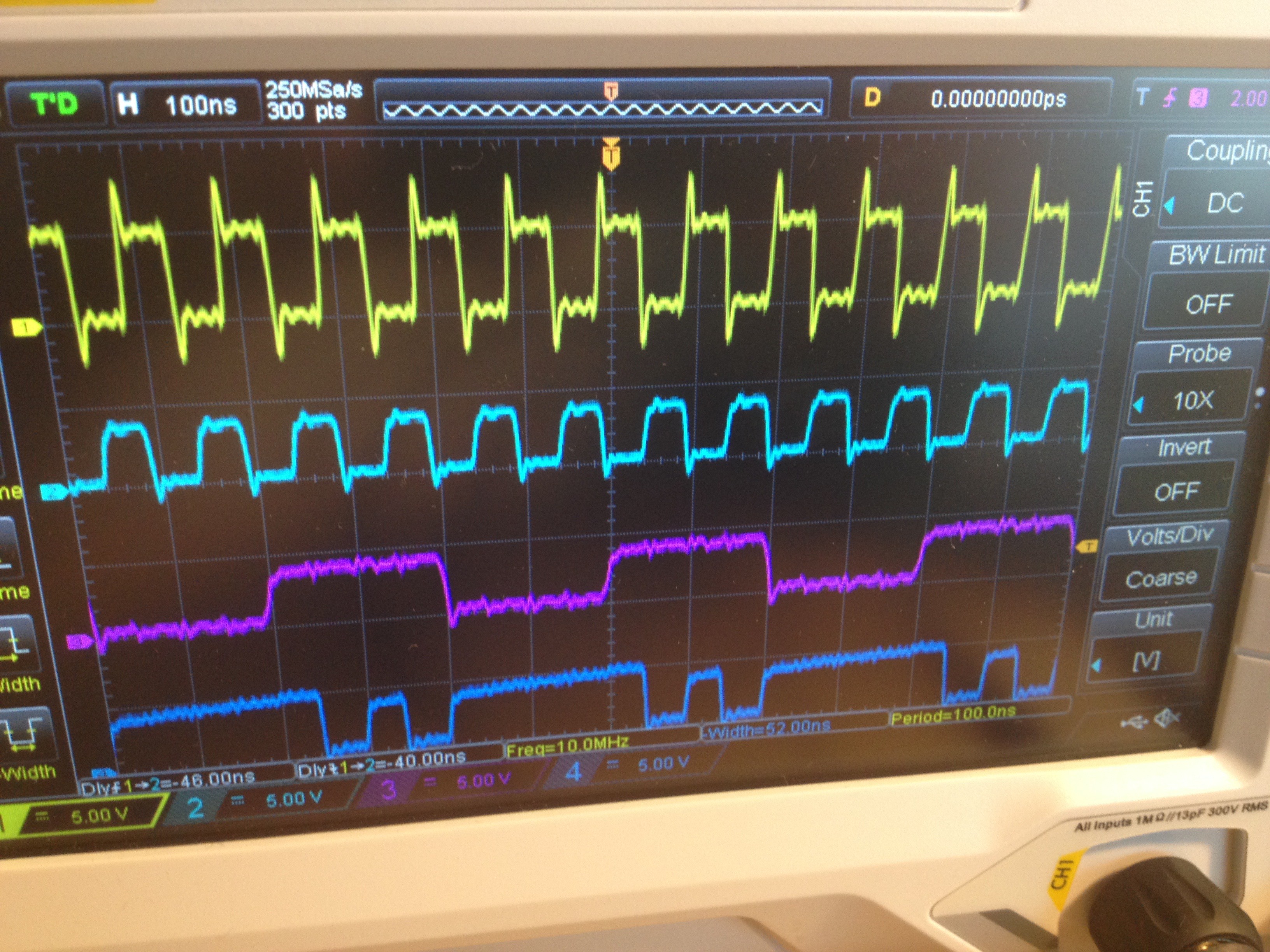
From left to right: 10 MHz clock, 74LS74 dual flip-flop, 74LS86 quad xor, 74LS273 register and a 74LS00 quad nand. Plus some probes. This is what we get:
![]()
From top to bottom: yellow = clock, cyan = inverted clock with clearly some phase shift, purple = simulated instructions (low is read, high is write), and blue = the resulting write-enable signal that must go into RAM.
It works! We see nice pairs of negative write pulses and no glitches. Even better, with a 10 MHz clock the write pulse is still over 50 ns wide. For the 70 ns RAM I intend to use the write pulse has to be at least 50 ns. I wonder if the rest of the system can keep up with that as well.
-
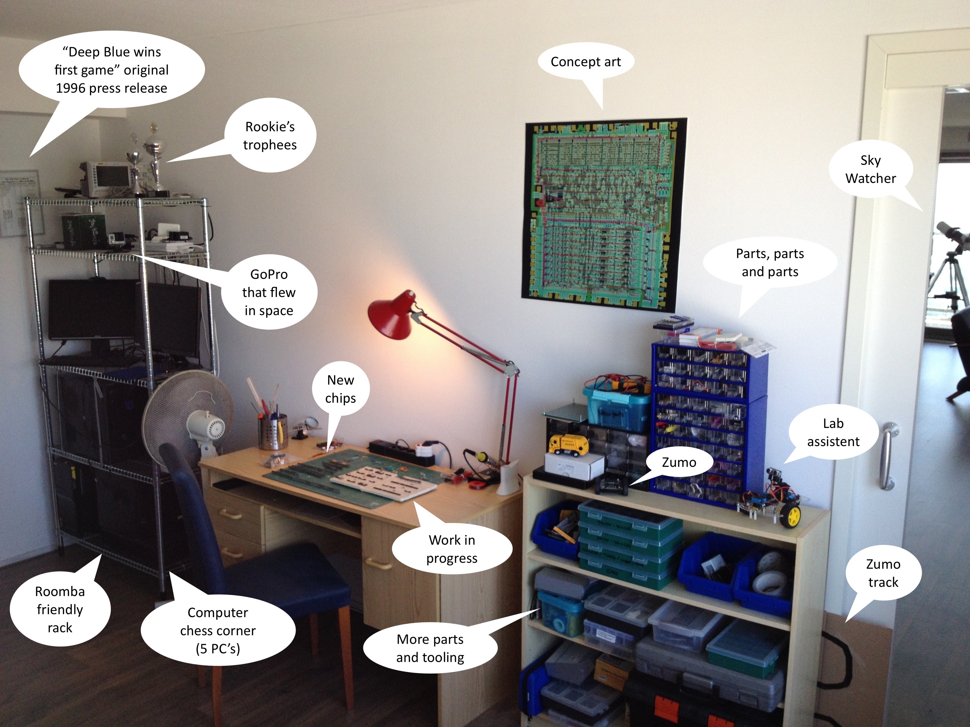
The lab
04/02/2017 at 11:21 • 6 comments![]()
This is what my geek corner looks like. Spring is in the air, so in the upcoming months I will spend more time on the balcony with a Chardonnay than here :-)
Gigatron TTL microcomputer
Just because! A home computer without microprocessor