Erik Piehl
-
Bug fixes and support for 512K cartridges
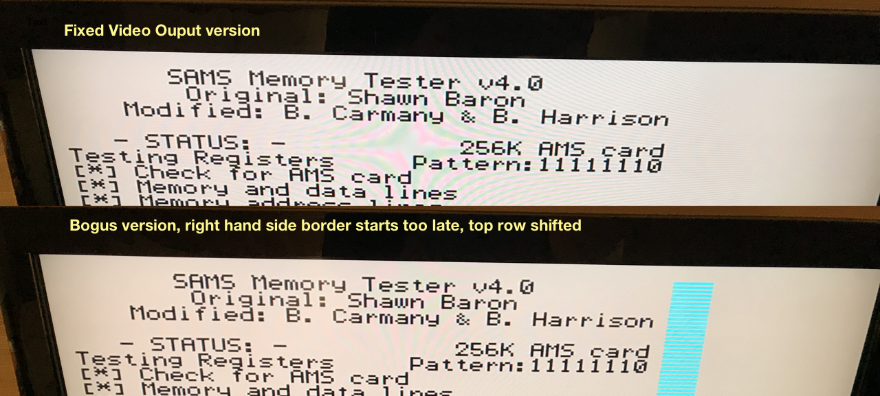
10/09/2017 at 14:58 • 2 commentsI did a couple of important bug fixes. I finally found, actually surprisingly quickly, the bug that caused the top pixel line to be shifted. The picture below illustrates this problem. The problem was not on the top line, it was that all the other scanlines of the picture that were right shifted by one pixel. This can be seen in the picture below, for example by looking at the top pixels of the M character on the topmost line.
I also modified the right border start setting to properly display border colour in 40 column text mode. In that mode the picture is 240 pixels wide, not 256 pixels as in all the other modes. Not dealing with this properly caused the VGA scanline doubler to show pixels that were not written to during screen refresh.
![]()
Then I changed the memory mapping, to support 512K cartridges. I did this by reallocating the 1MB external memory to Ti-99/4A mapping. Now 512K is allocated for paged cartridges (up from 64K). That came at the expense of reducing SAMS compatible memory to 256K. But importantly this allowed me to run the cool TI-99/4A megademo called "don't mess with Texas", and running that demo did reveal some bugs, below is the video.
-
Speed control needed - and added
09/20/2017 at 21:30 • 0 commentsI wanted to continue my benchmarks and run my simple Basic program also under TI Extended Basic. That turned out to be impossible, as the keyboard repeat rate problem was much worse under extended basic than built-in Basic.
It was time to do something about this. Instead of trying to hack the code (I tried quickly but too much code to disassemble and understand) it was time for a hardware solution. Execution speed on the TMS9900 is largely dependent on memory access speed. I added a 6-bit delay counter, which enabled me to add up to 63 wait states per memory access. The Pepino FPGA board has a 8 DIP switches, so I used three of those switches for determination of wait states (I did this with a clocked latch, so it is possible to adjust speed in flight):
- DIP switch 1 on: 63 wait states
- DIP switch 2 on: 31 wait states
- DIP switch 3 on: 8 wait states
- All off: no wait states
Switch 1 has priority, so if it is on there will be 63 wait states. I also took a quick look at the CPU's memory timing under simulation: with no wait states reads take 40ns and writes 60ns, with 63 wait states reads take 670ns.
Alas, it turned out that a 6-bit delay counter was too short, as I got these results when comparing execution speed under TI extended Basic for my test program:
- Classic99 emulation: 1 min 11 s
- 63 wait states: 24.7s, 2.9x faster
- 31 wait states: 13.6s, 5.2x faster
- 8 wait states: 5.6s, 12.7x faster
- 0 wait states: 2.9s, 24.5x faster
So even with the maximum of 63 wait states this thing goes too fast... Need to slow it down further. But not tonight.
Here is a video:
-
Nearly doubling the performance - 23x original TI-99/4A
09/17/2017 at 20:44 • 1 commentI started to see how I could optimize the CPU.
I looked at my memory interface code in the TMS9900 core, and realized I have been using very conservative timings - just to make sure that when debugging the CPU the memory interface does not cause problems. But now it is time to optimize!
My TI Basic test program:
10 for i=0 to 1000
20 print i;" ";
30 next i
Takes 160 seconds on a standard TI, and 11.6 seconds on the previous version of the CPU.
I tweaked CPU memory interface first on the read side, reducing the number of wait states.
That took me from 11.6s to 8.9s, and then after further tweaking the execution time dropped to 8.2s. This just by reducing the wait states on the read side.
Next I reduced the number of wait states on write side. This brought down the execution time to 7.7s. The impact of reducing write states on the write side is much smaller than on the read side, since the CPU mostly reads data and seldom writes it.
After these changes I removed one extra "safety" state after each read (it was just there to make sure the bus interface has some time to settle after reads, but that is not really necessary as the main state machine anyway adds a delay cycle). That brought the time down to 7s. With these changes the execution time is only 60% of what it used to be! And the speed is now 22.9 times of the original TI.
As a final tweak I removed one extra "safety" state that was there after each write - for the same reason as the read cycles. That reduced run time to about 6.8s, so now the CPU runs my benchmark 23.5 times faster than the original TI.Here is Parsec running at this new revised CPU:
When doing these tests, I really appreciated the quick re-synthesis time, it only takes my PC a couple of minutes to do the synthesis, so test iterations are fast.
I also took a look at how much FPGA capacity the current design takes - it takes 51% of the LUTs (look up tables), so there is plenty of space left. Also there is some debug features included in here, removing those would make the design smaller. -
The keyboard repeat rate problem and fix
09/17/2017 at 19:45 • 2 commentsIf you looked at the video I posted on previous project log, you saw that I had great difficulty in typing in Basic programs because keyboard repeat rate was just crazy when CPU was running at 15x speed.
I decided to tackle this problem, by reading the TI ROM code from the excellent book "TI Intern". Page 21 looked promising, there was was some kind of keyboard scanning routine delay:
Time delay routine at >0498
0498 LI 12,>04E2
049C DEC 12
049E JNE >049C
04A0 B *11Unfortunately changing the above did not help, I modified the counter from >04E2 to >024E2, but this did not help.
After a little more searching (just for the word repeat in the book), I found a more promising piece of code. This time it was not in the Basic ROM, but in Basic GROM. GROM contains code in the interpreted GPL language, not TMS9900 machine code. I don't really know too much about GPL, but hey let's try changing it and see what happens:
Page 149 and 150 talk about repeat counter GPL code. Memory location >830D is set to zero and when it exceeds >FE, repeat occurs. After repeat that location is decremented by >1E (or this is what I think the GPL code is doing). So the next attempt is to change the GPL code
2A6B SUB @>830D,>1E
to a larger subtract, so that repeat would be slower. This actually helps! But the range is too small and sporadic repeats still occur, even SUB >FE is not enough. The parameter is byte sized, so I cannot subtract more than that. The FPGA CPU just goes too fast and the counter gets incremented from zero to FF too quickly.Then I got another idea: What if I could disable the repeat code altogether? At 2A4F there is CLR @>830D and it is a two byte opcode, just the same length as the INC opcode at 245F which is taking care of counting the repeat up.
What if we just copy the CLR opcode to 2A5F, overwriting the INC? Then key repeat counter never increments, and we should never get into trouble, right?
2A4F contains 86 0D and this must be CLR @ opcode.
2A5F contains 90 0D and this must be INC @ opcode. So I'll just put 86 in 2A60 and hope for the best.That worked! No more repeats and keyboard is usable under TI Basic. The downside of this fix is that while it helps with TI Basic, I don't know if it helps in other programs such as TI Extended Basic, which may use their own code for key repeat - I guess I will see.
-
Success! FPGA based TI-99/4A working!
09/17/2017 at 07:41 • 1 commentFinally I got my TMS9900 CPU to work enough that I can run original TI-99/4A software on my FPGA based TI-99/4A clone. Below you can find a link to my quick-and-dirty but rather long video about the whole project.
Prior to this last working session I knew that I still needed to implement the divide instruction, so I went about doing it. I did that by first writing a very simple C program, and then converted that functionality to VHDL.
unsigned short tms9900_div(unsigned int divident, int divisor) {
    unsigned short sa;      // source argument
    unsigned short da0;     // destination argument (high 16 bits)
    unsigned short da1;     // destination argument (low 16 bits);
    printf("divident: %d divisor: %d\n", divident, divisor);
    // algorithm
    da0 = (divident >> 16);
    da1 = divident & 0xFFFF;
    sa = divisor;

    int st4;
    if (
        (((sa & 0x8000) == 0 && (da0 & 0x8000) == 0x8000))
        || ((sa & 0x8000) == (da0 & 0x8000) && (((da0 - sa) & 0x8000) == 0))
        ) {
        st4 = 1;
    } else {
        st4 = 0;
        // actual division loop, here sa is known to be larger than da0.
        for(int i=0; i<16; i++) {
            da0 = (da0 << 1) | ((da1 >> 15) & 1);
            da1 <<= 1;
            if(da0 >= sa) {
                da0 -= sa;
                da1 |= 1;   // successful substraction
            }
        }
    }
    printf("quotiotent: %d remainder %d st4=%d\n", da1, da0, st4);
    printf("checking: quotiotent %d remainder %d\n\n", divident/divisor, divident % divisor);
    return da1;
}
Getting this algorithm implementation to work took something like 15 minutes, so this was quickly done. Also the VHDL implementation did not take long, although I did manage to bring a few bugs. I had been delaying a little the implementation of the divide instruction since I thought it would take a long time, but actually that was quickly done.
After implementing the divide instruction it was not smooth sailing yet, since keyboard was not working properly. I traced the problem to the CRU interface (LDCR and STCR) instructions. STCR which reads from the external CRU and writes to a destination, returned bit shifted data. As an example, the expected value for button '1' in my test program would have been >FEFF, but the read data was >FDFF, so there was a shift of one bit. I did run multiple simulation runs with my VHDL test bed, but it always worked. Finally after some head scratching this turned out to be a major timing error: the STCR instruction presented the address to read from on the first cycle, and already on the 2nd cycle following it (i.e. 10ns later) it was latching the data. Inside my FPGA TI-99/4A implementation that was way too fast, so I added a two clock cycle delay before sampling the CRUIN pin - and voila, my TI-99/4A clone was running!
The performance however turned out to be slower than expected: it only runs 15 times faster than the original TI, despite a 30 fold difference in clock speed (3.3MHz vs 100MHz). When I was creating the TMS9900 core my first priority was to get the bloody thing running, so I did not pay much attention to how many states each instruction has to flow through to implement it's task. I do like to optimise though, and now that my TI clone is working, I can turn my attention to make it running even faster :)
Source code can be found here:
Link to GitHub (the FPGA CPU is in the soft CPU branch).
And here is the video talking about the project a bit:
-
Almost there!
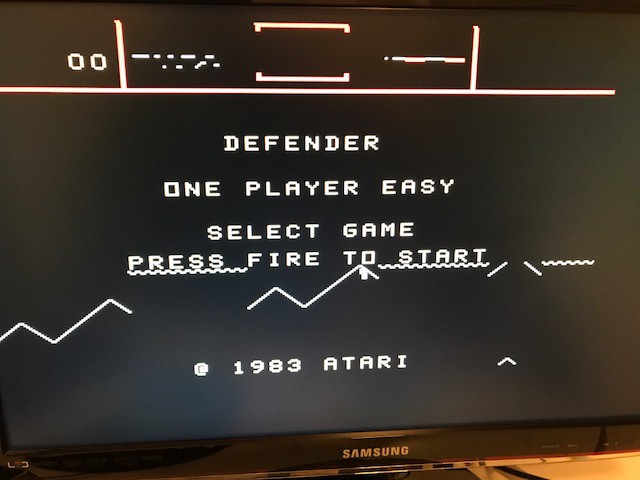
09/13/2017 at 20:26 • 1 commentAfter extensive debugging and comparison of execution logs between the FPGA CPU and the results of Classic99 emulator with the same ROMs, I found and fixed four bugs, one of them being quite nasty to find. But the results were very pleasing, now with my own boot ROM and Defender cartridge loaded I get this picture (story continues after the picture):
![]()
For the first time the FPGA CPU renders the opening screen correctly! Interrupts were disabled (at hardware level) for this run.
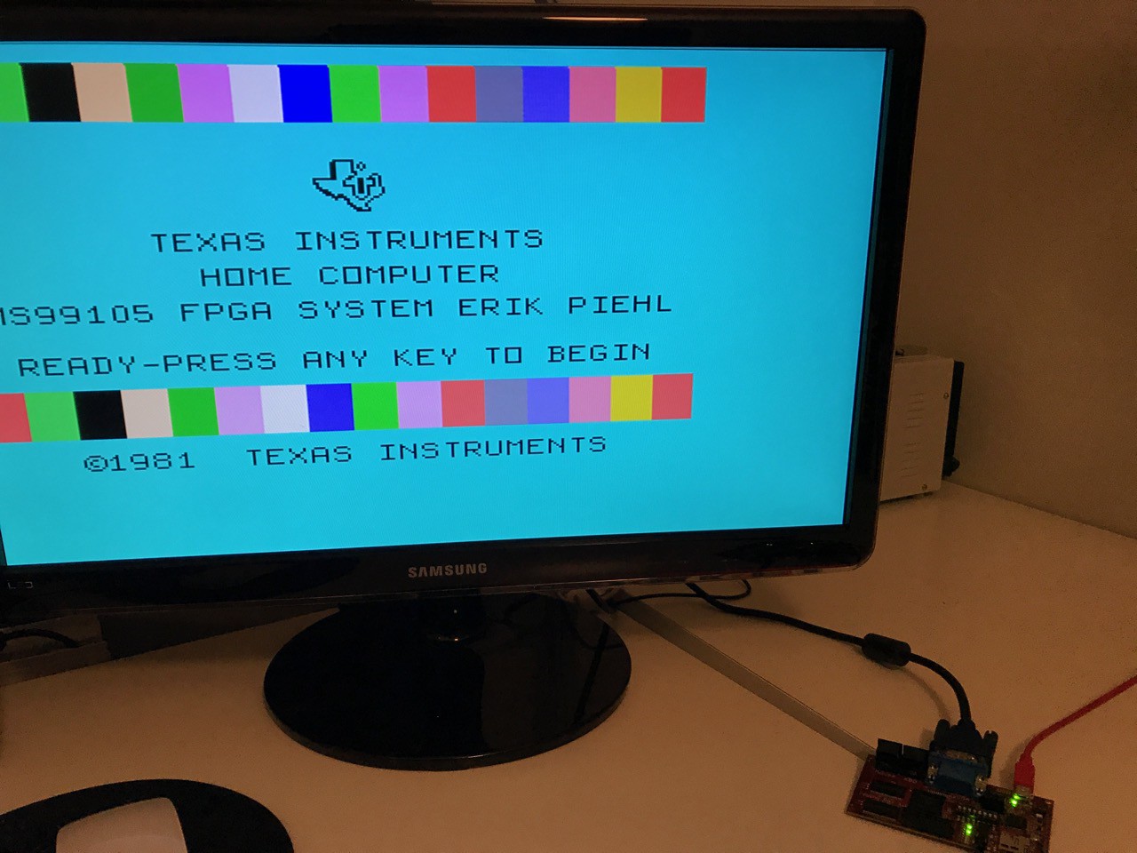
Even more pleasing, I tested the bug fixes with the normal TI-99/4A ROMs, and got this boot picture for the very first time (story continues after the picture):
![]()
Personally this was a wow moment!
So what were the bugs? Three related to flags, and one to addressing modes:
- The logical greater than flag (ST0, also known as L>) was set incorrectly for the compare instructions (C and CB). Similarly the arithmetic greater than flag (ST1, also known as A>) was set incorrectly. I did not find this bug in the past, because in many scenarios the flags were set correctly. I had read sloppily the data sheet, and in the VHDL code I was had accidentally swapped the source argument and destination argument inputs in the flag setting code when comparing their MSBs to detect certain conditions.
- Related to the above, my flag setting code treated comparison (C and CB) and subtract (S and SB) instructions identically. For most CPUs this would be true, but for the TMS9900 family the aforementioned flags ST0 and ST1 rather strangely only compare against zero for the subtract instruction. So I modified the code to properly distinguish S and C instructions, this required a number of changes.
- In the data sheet The carry flag ST3 is documented for subtract instruction to be set when "CARRY OUT" is set. However, "CARRY OUT" is not defined anywhere. I used simply ALU output bit 16 (i.e. the 17th bit of the ALU) as carry. This is fine for addition instruction, but subtract actually inverts that bit. I guess in the original CPU implementation this was the most effective way to implement the ALU (normally done by inverting the number to be subtracted, tweaking carry so that an "add" operation becomes a "subtract").
- Hardest of all to find, I could not understand why the compare bytes instruction "CB R5, @>6049" in the defender game cartridge set flags incorrectly with my FPGA CPU. I modified my boot ROM to run this instruction among the very first instructions, so that I could check the behaviour both under simulation and actual FPGA by running only a few instructions - and it worked properly. But the same instruction much later on - as instruction 11 460, did not set the flags properly. This was a very hard bug to find, but I finally found the problem after adding ALU input debug registers and making them available for my debug software. I could see that in the latter instance this instruction was producing different ALU inputs, despite the actual inputs being exactly the same. I finally traced down this problem to the operation of the byte aligner. It used an internal register simply called "EA" for effective address to perform the alignment of input bytes i.e. conversion of an input byte to 16-bit ALU input. Now this register was not set at all if the source operand was a register operand, i.e. in this case R5. Thus the byte alignment was random and depended on whatever code was being run before. The problem was actually generic to all instructions in the TMS9900 instruction set that used byte operands.
After fixing all of the above the FPGA CPU runs the TI99/4A boot ROMs and renders the familiar boot picture! It then stops at address >0296 where it finds the opcode >3D06. This is a divide instruction, and the FPGA CPU does not support it yet, but rather simply stops and leaves the program counter pointing at the unimplemented instruction, making the problem easy to spot. I knew that this instruction was still not implemented, so I was happy to see that the reason for the CPU halting was the "right" one. Hopefully after implementing this last thing the CPU fully works and finally marks the implementation of the entire TI-99/4A computer on the FPGA!
-
Debugging with Defender
09/06/2017 at 19:22 • 1 commentWow it's been a really long while since I posted the last update here! Well, I have not given up on this project - quite the opposite. It's just that I haven't had time to work on this project in a long while. To my delight there have been more followers to this project in the mean time, so it is about time to show a sign of life.
I have not done too much progress since the last update, the only thing I've done is adding more support for debugging. Now when single stepping I record more information than in the past:- Program counter
- Address of last write to memory
- Data of last write to memory
- Status register contents
This stuff goes into a log file, the data is written by the Windows program running on the PC which controls the single stepping of the FPGA CPU. Basically it lets the CPU to step one instruction, then it reads the above data (below an example) and the continues with the next instruction.
line:pc  :addr:data:st
   1:0028:83FA:9800:8DC0
   2:002C:83FC:0100:CDC0
   3:0030:83FE:8C02:8DC0
   4:0034:83E0:0020:CDC0
   5:005C:83E0:0020:CDC0
   6:005E:83E8:0000:29C0
   7:0060:83EC:0020:C9C0
I compare this output of the FPGA based CPU to the output of the famous classic99 emulator (I modified the emulator to record the same stuff). Then I wrote a python script to compare the two files. This comparison cannot be done with a normal diff tool since there are some acceptable differences (for example my CPU sets the unused flag bits differently from a real TMS9900).
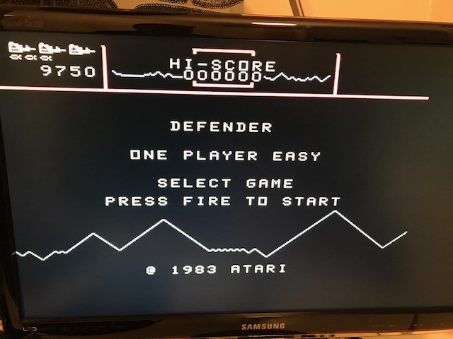
In the past I've tried to do the analysis with TI ROMs, but unfortunately that doesn't produce any output before the FPGA gets stuck somewhere after running correctly a large amount of instructions. Capturing the single step log is a slow process, due to the number of USB transactions needed - my debugging implementation is not that great in that respect. So I now decided to go with another strategy: rather than using the TI Basic ROMs, I'm trying to use the Defender game cartridge. Instead of the normal TI Basic routines firing up the game, I start the game "by hand" using a minimalistic boot loader. With the FPGA CPU that produces the following picture:
![]()
This clearly is bogus as can be seen. For reference, my other FPGA project which uses a real TMS99105 CPU chip produces the following picture with the same ROMs loaded:
![]()
So the positive thing is that the FPGA CPU does quite many things right... Now I need to load this boot ROM / defender combination to classic99 and capture the log and then make the comparison. For that I need to find out how to load my custom ROM in classic99 instead of the normal Basic ROM...
My motivation to use the defender game cartridge also comes from the fact that this game cartridge contains only a normal ROM chip, not a ROM + GROM combination. I hope that simplifies matters in debugging, as it should mean the GROM interface does not have to work perfectly for the game to work. The fonts seen in the pictures above are loaded from GROM to video memory by my boot code, so the GROM data is still initialised.
Stay tuned, hopefully for not too long this time, as I am trying to make progress with debugging. With this long pause it takes a while to get back up to speed. Luckily I've become pretty good at taking notes - I can't trust my memory to serve me right in projects like this, with pauses of several months between work sessions.
-
Some fixes and debugging features
05/29/2017 at 20:46 • 0 commentsNot much progress in the last week or so, but something still. I've been trying to get the TI-99/4A ROMs to run on my CPU, but no luck yet.
X instruction
I found a bug in the implementation of the X instruction. One memory read was missing from the execution state sequence, and caused the instruction to essentially execute a random opcode. The X instruction is certainly a very CISCy instruction, it allows one to execute a single word instruction provided as an operand. Very different from the normal case where instructions are fetched from the program counter, here one can write "X R5" to cause the CPU to execute the opcode stored in register 5. The X instruction was an instruction I did not test, but subsequently learned it was used by TI-99/4A ROMs. Of course there was a bug in implementation...
Single stepping
The way I found the bug in the CPU was such that I modified the classic99 emulator so that it outputs instruction traces, namely the values of PC and ST registers before each instruction execution. These are stored in a text file. Then I modified the FPGA CPU so that it has single stepping capability: one control register bit enables single stepping mode (effectively by just asserting a DMA request making the CPU stop), and another control register bit, when set, briefly releases the DMA request so that the CPU starts to execute an instruction. DMA request is then immediately asserted again, but my CPU implementation only samples DMA requests during opcode fetches. Together those features enable single stepping. I then added a 64-bit debug register, which is readable over the USB connection. In that register the values of the current opcode, PC and ST are available. That way I could create a similar trace of instructions as in the emulator run. I extended my host side Windows program to have this feature.
Doing single stepped instruction trace comparisons enabled me to see the differences in behaviour, and I found that the X instruction was bogus. Unfortunately this method only goes so far, since there are vast timing differences. Single stepping is done with PC control and runs very slowly due to that, so once interrupts are enabled the comparison method no longer works, as interrupts are served way too slowly and therefore are always pending. Once the CPU exists the interrupt service routine, it just jumps right back in. I guess I may have to add an additional interrupt debug mask bit to disable video processor interrupts during single stepping runs.
Byte wide instruction flag bug
My VHDL code has a process which computes byte alignment, i.e. when the CPU is reading a byte from memory, this block aligns it properly as a 16-bit entity. This is done by zero extending and moving the desired byte to the most significant byte of the 16-bit operand word. Yes, this is different from x86, byte operands are not handled by the TMS9900 as the least significant bytes of registers, but as most significant bytes. A mindset difference right there.
By comparing instruction traces I noticed that sometimes my FPGA CPU was setting status bits incorrectly, and after some pretty intensive testing I realised that if the source operand of a byte wide operation was a register (not memory location) the zero extension did not work, but instead the entire 16-bit contents of a register were passed to the ALU. The correct operation is to only pass the high byte of the register and zero out the least significant byte. This was difficult to find since the actual operation (datapath) worked correctly, only flags were sometimes set incorrectly due to the LSBs having some non-zero bits. Now this is fixed. The bug was not there if the source byte was read from memory (for example by indirection such as in MOVB *R2,@>1234). I am sure there is a ton of nasty bugs like this one left to debug. But one more down!
-
MPY and flag fixes
05/21/2017 at 06:37 • 0 commentsReal life has kept me busy... I did a few small tweaks to the TMS9900 core: I added support for the MPY (multiply) instruction. I also started to implement CPU status flag support more carefully, and implemented a few changes to the handling of ST0 (Logical Greater Than) flag, as well to the handling of ST1 (Arithmetic Greater Than) flag. ST0 is the MSB i.e. bit 15 of the status register, while ST1 is bit 14. For whatever reason the TMS9900 generates these flags in what seems to be an inconsistent way: for both flags the "correct" behaviour is only done with the compare instructions (C, CB, CI). With other instructions (except special handling of ABS instruction - I did not implement that yet), the flags become simpler and mostly just versions of "non-zero" flags.
The multiply instruction I implemented with Xilinx Spartan 6 hardware multiplier, so this instruction (while not optimized) has a much higher performance than on the original CPU. Reading the data sheet the multiplier can compute the multiply operation in 3 cycles - it could do it even faster in pipelined mode but that is neither necessary or useful on this CPU core.
I have three test programs that I use for testing: the original TI ROMs, my custom boot loader and a instruction test program I use for simulation. My custom boot loader has the ability to start the Defender game, if the ROM image for that cartridge has been loaded. Both of my own test programs work, but the TI ROMs still do not work. With the changes to the handling of flags, now the Defender cartridge image renders the first screen before somehow crashing. So some progress, but still no beef yet.
-
Interrupts now work
05/16/2017 at 20:59 • 0 commentsOne more feature done! Now the CPU core supports interrupts, leaving the major missing features to MPY and DIV instructions - and a whole bunch of debugging.
The CPU core now has 3 more I/O signals:
int_req : in STD_LOGIC;         -- interrupt request, active high
ic03     : in STD_LOGIC_VECTOR(3 downto 0);     -- interrupt priority for the request, 0001 is the highest (0000 is reset)
int_ack : out STD_LOGIC;
Of these on both my simulation framework and the actual FPGA implementation I set ic03 bit vector to "0001" so all interrupts occur at the highest level. This is how interrupts are hardwired on TI-99/4A.
int_ack is a signal that does not exist on the real TMS9900 CPU. In my case it is set to high while the CPU fetches the new workspace pointer from the interrupt vector table. This would allow external hardware to see that the CPU is vectoring to an interrupt, and also which interrupt it is. Maybe the actual CPU does something similar, but this was simple so I did it... At least useful for simulation runs.
It is amazing that there is almost no feature where the first implementation version wouldn't have several bugs: in my case when the CPU vectors to an interrupt it needs to modify its internal interrupt level (stored in 4 LSBs of the status register). I managed to implement two bugs in there first: initially I latched the interrupt priority code too early, so that when the CPU exited the interrupt service routine, it actually remained at a higher interrupt priority level than before the interrupt, because I altered interrupt priority before the previous level was stored to memory (as part of status register). So a flag bit was needed to modify the status register's interrupt priority field only after storing the previous contents to memory as part of the interrupt context switch.
The second problem was harder to debug, since it only occurred with FPGA run and not on simulation. When the CPU vectors to an interrupt, it must also adjust the current priority level not to the level that external hardware is requesting the interrupt for, but to a level below, as to block the same interrupt from firing over and over again. The following code does the right thing in the processing of the do_blwp3 state (this is part of the chain of states the CPU execution state machine marches through when entering the interrupt):
if set_int_priority then
  st(3 downto 0) <= std_logic_vector(unsigned(ic03) - 1);
  set_int_priority <= False;
end if;
So a four bit decrementer is required to compute the new interrupt priority.Having interrupts working both in simulation and on the FPGA allowed me to also properly implement the IDLE instruction. This instruction simply waits for an interrupt. I added a new state to the CPU, which waits for an interrupt that has the same or higher priority that CPU currently has.
On the TI-99/4A hardware that my FPGA implements the interrupt originate from my TMS9918 video processor core on every frame, then pass through my TMS9901 core which further can mask the interrupt, and finally it goes to the CPU core. Thus on the TI-99/4A clone the IDLE instruction (assuming the video processor and I/O controller are properly set up) becomes a wait for next video frame operation.
TMS9900 compatible CPU core in VHDL
Retro challenge 2017/04 project to create a TMS9900 compatible CPU core. Again in a month... Failure could be an option...