Erik Piehl
-
First successful run
05/15/2017 at 21:22 • 2 commentsAfter some debugging I got the TMS9900 CPU core to run on the FPGA chip. That's very cool! Even in this completely unoptimised form it runs a fair deal faster than the TMS99105 processor shield I built before. The CPU core is not yet fully functional, it lacks interrupts and DIV/MPY instructions, but I can run my demo code on it. The demo runs equivalently on the new CPU core as it did on the actual TMS99105 chip:
I also tried to run the full TI-99/4A on it (as the peripheral set is the same), but it wants to go to never-never land. That is hardly surprising, as I have tested the CPU very little. It actually is more surprising that it does run the demo code correctly. That program has about 650 lines of assembly code, and it does exercise a fair amount of instructions - and interfacing to the TI-99/4A hardware on the FPGA chip, namely the interface to my TMS9918 implementation. That part of the code loads up fonts to the video memory of the TMS9918.
Before I was able to get this far I needed to integrate the TMS9900 core in a functional way to the rest of the logic I created earlier for my TI-99/4A clone. I had a bunch of difficulties in getting the CPU to run. Eventually I added debug registers to help me figure out what was not working. The CPU core component exposes a 48-bits wide debug bus, which contains three 16-bit fields:
- The opcode of the very first instruction fetched from memory
- The value of program counter +2 where the last instruction was fetched
- The opcode of the last instruction that was fetched.
I also added another 64-bit debug bus to my top-level VHDL module, which connects to the SRAM memory bus (my TMS9900 core uses the external SRAM as its memory, it does not use any internal block RAM). This 64-bit debug bus contains the 16-bit CPU address bus, the 18-bit SRAM address bus (there is a memory paging subsystem, and a bus multiplexer to connect to the 32-bit wide SRAM bus), a few status flags, and the last 16-bits read from the memory bus.
The beauty with the debug buses is that they are exposed through my USB memory controller interface, allowing me to see what the contents are. Normally those values would be flying by, but when the CPU core hits an opcode it does not understand it will enter a "stuck" state, and light up a LED. That allows me to see that it got stuck, and by reading the debug buses I can see what is wrong. That is the theory at least. It did help me debug the SRAM memory interface, so that my CPU core could read and write memory reliably. But when running the normal TI-99/4A ROMS, I can only see that the CPU gets stuck in a memory location it is not even supposed to fetch instructions from... That is not surprising.
But the nice thing about working with FPGAs is that I can next equip my CPU with more debug features - it seems it would be very useful to have a trace buffer, where I could store for example the last 1024 or so instructions and their addresses. I could also force the CPU stuck the minute (eh nanosecond really) it starts to execute instructions from a memory location it is not supposed to run code from.
-
CPU was synthesis passed!
04/26/2017 at 20:24 • 0 commentsI wrestled today with two of the remaining instructions, LDCR and STCR, but before explaining them, I did plug in the CPU to my EP994A project (TI-99/4A clone), basically replacing the external TMS99105 interface - and synthesis did pass!!!!!! Wow! I did a really stupid integration, just wiring signals in there in a semi logical way, as to force the logic synthesis to do something - and it did! The very first attempt succeeded! It will not work for sure, as the bus interface I created is different from the TMS99105 - it has vastly different timing, so I need to modify the integration logic quite a bit.
But here is the interesting stuff, a comparison of how many logic resources were consumed on the Xilinx XC6LX9 FPGA, with "only" the TI-99/4A logic, and with the logic including the CPU (granted the CPU is bogus and the integration even more bogus - but we don't care, the ballbark is what matters):
TI-99/4A + external TMS99105 TI-99/4A + new TMS9900 core Number of slice registers used 966 1248 Number of slice LUTs 1402 2663 Number of slice LUTs % 24% 46% LUTs used as logic 1381 2636 LUTs used as memory 9 14 Occupied slices 36% 64% I like these results :) It means that the FPGA easily accommodated the CPU implementation with the rest of the TI-99/4A logic. In fact even if the CPU is totally bogus and much more logic is required, it will fit in. In fact on this relatively small FPGA there is enough space to add at least one more TMS9900 core. Also the instruction decode etc. is completely state machine based, so it does not use any of the memory blocks of the FPGA. The CPU could be partially microcoded by using a memory block to save logic if necessary.
Of course a working integration of the CPU will change the numbers - but integrating the on-board CPU is actually more straightforward than interfacing to an external CPU. And if it becomes complex I can always modify the CPU bus interface...
Still DIV and MPY instructions are not implemented, but I think I will next focus in getting the CPU integrated so that I can actually prove that it works in the FPGA implementation. This could be a lot of work...
LDCR and STCR instructions
Before doing the synthesis I spent quite a bit of time of implementing and simulating two of the remaining four instructions:
- LDCR - "load control register" i.e. write serially data to an external device
- STCR - "store control register" i.e. read serially data from an external device
They were both nasty instructions to make. The bit serial CRU interface on the TMS9900 uses the address bus to tell the external world which bit is addressed. When writing or reading more than one bit - which is pretty much always the case with these instructions - the CPU must increment the address and shift bits appropriately. It also needs to separately handle transfers between 1 and 8 bits, and 9 and 16 bits. Between 1 and 8 bits the CPU operates in "byte mode", so for example when using the auto increment addressing mode:
LDCR *R3+,5
Writes 5 bits from the address pointed to by R3 and it auto increments R3 by 1. But if the bit counter is higher:
LDCR *R3+,9
The auto increment is by two. This gets more hairy with the opposite direction, for example with
STCR *R3+,5
This will read 5 bits and do a byte write to the address pointed to by R3. Since the external bus is 16 bits wide, the CPU actually must do a read-modify-write cycle and modify either the low or high byte (depending on the LSB address bit).
To make things a little more involved, the number of bits transferred is encoded into 4 bits, with the value 0000 indicating 16 bits. So that needs to be handled properly too.
My implementation seems to do the appropriate things now, based on my limited experience of running on the real iron and reading the data sheet. The data sheet is really not verbose as to how these instructions work. The instructions also mess around with flags, but I did not implement that support yet.
-
3 more instructions
04/25/2017 at 20:39 • 0 commentsToday was a busy day in the office - I just had the time and energy to add 3 more instructions. They are from a new category - one that only allows a workspace register as a destination parameter, while the source operand can have all addressing modes, for example:
- COC R4,R3
- CZC @TABLE(R2),R3
- XOR *R7+,R2
This category has five instructions in total (DIV and MPY are still missing) but COC, CZC and XOR are now done. Of these instructions XOR is the most familiar and supported by virtually all processors - it just does the XOR operation of source and destination and stores the result to destination while also setting 3 status flags.
COC and CZC are unusual instructions, I have not seen these on any other processor although I have programmed in assembler on many CPUs.
COC stands for "compare ones corresponding" and CZC stands for "compare zeros corresponding". Since they are comparison instructions, there is no actual data output other than the result of comparison which is stored in the zero flag.
I implemented both using new ALU operations, in VHDL as below. I don't think I have ever used these instructions, so this implementation follows from what I understood from the TMS9900 data sheet.
COC: alu_out <= ('0' & arg1 xor ('0' & arg2)) and ('0' & arg1);
CZC: alu_out <= ('0' & arg1 xor not ('0' & arg2)) and ('0' & arg1);
(The extra zero bits '0' are just garbage in the above to account for the fact that the ALU is actually 17 bits wide, in order to be able to generate the carry flag - which is not used by these instructions).
Both of these comparison instructions take the source operand (arg1 above) and make sure that the result indicates that in the destination operand there are one bits (for COC, or zero bits for CZC) in each location where there are one bits for the source. I did the core of the comparison with XOR, and arg1 is used as a bit mask to leave only the relevant bits. The standard result comparison to zero in the flag creation logic works.
I'm not really sure why they thought around 1977 that these are useful instructions... I can only assume they originated from the minicomputer architecture. These operations can so simply be implemented with basic boolean operations. Clearly this architecture was not designed with C compilers in mind - but that is evident from many other things as well, such as the lack of a proper hardware supported stack.
Whatever - 3 more instructions done and a little tested - and only 4 instructions remain!
-
XOP, STST and external instructions
04/24/2017 at 20:31 • 0 commentsI was hoping to complete the core in terms of instruction set today - but no such luck. But I did add a bunch of instructions:
- XOP - extended operation. More about this below.
- STST - store status word to a workspace register. I am kicking myself for not implementing this instruction before, as it enables very easy flag functionality verification: do a computation impacting flags, store flags into a register and do an immediate comparison. If mismatch, stop. The source material for the comparison needs to come from a genuine TMS9900 or more likely from the classic99 emulator - or from my TMS99105 based TI-99/4A clone. This should be an easy way to verify the behaviour of flags which is pretty involved on the TMS9900.
- STWP - store workspace pointer to a workspace register.
- IDLE, RSET, CKOF, CKON, LREX - These are so-called external instructions. They basically just show a status code on the bus. IDLE should also stop and wait for an interrupt but I am not doing that yet.
The XOP instruction turned out to be the real deal, a proper mega instruction. I was thinking earlier after adding the BLWP instruction, that it does not get more complex than that. The XOP is a kind of software interrupt, which transfers control via a table in address >0040. What is unique about the TMS9900 is that the XOP instruction support a parameter, and the effective address of the parameter is put into register R11. This really converts the instruction into a door to many useful and compact constructs. It is sad that in the design of the TI-99/4A ROM they did not really provide any provision for general use of this instruction.
An example: XOP *R3,3
This instruction activates the XOP number 3 (out of 16). The vector is calculated as >40+4*3, i.e. from >4C. From [4C] is loaded the new workspace pointer and from [4E] new program counter. Then no less than four values are stored into the new workspace: old values of PC, ST and W register, and finally the effective address of *R3 (which happens to be the contents of R3 which in this case would be a memory pointer).
I modified the processing of BLWP instruction to serve Reset, XOP and BLWP use cases - I suspect that once I implement interrupts they will also use the same internal states, since interrupts are effective a bit like XOPs or BLWPs, in that they also vector through a memory location, change context and save previous state into the new context.
After these instructions there are only seven instructions left to do! They are COC, CZC, XOR, MPY, DIV, LDCR and STCR. Of these I want the multiply instruction MPY to use the Xilinx FPGA DSP block for good performance. In addition interrupt support needs to go in, but that should be easy at this point due to the BLWP/XOP support.
-
BLWP, RTWP, Shifts and single bit I/O
04/23/2017 at 20:07 • 0 commentsOk so more progress for today. I implemented many key (unique but a little obscure) features of the TMS9900. Still testing under simulation. I decided to postpone actual hardware synthesis until I have all the instructions somehow implemented. After these additions there are not many instructions missing anymore.
- Now the core can process the most complex TMS9900 instructions, BLWP and RTWP.
- I also added all shift instructions SLA, SRA, SRC and SRL. These are fairly standard shift instructions as can be found in most processors.
- The TMS9900 architecture has a unique serial I/O facility called the CRU interface. This interface supports single bit and multiple bit transfers, using 5 instructions overall. Now the core implements the single bit variety, with SBO, SBZ and TB instructions. The multiple bit instructions are not yet there (LDCR and STCR).
I tested all of the above in simulation. Not comprehensively, especially regarding flags. But BLWP and RTWP work - I actually changed reset processing so that reset is done by forcing a BLWP from address 0. BLWP does a ton of stuff:
- It has a source operand, which supports the normal slew of addressing mode.
- Once the effective address of source operand is calculated, two 16-bit words are read from there: the new workspace pointer and the new PC.
- As the CPU enters the new workspace, it saves the entire context of the CPU to the new workspace by writing old WP to R13, old PC to R14 and old flags (ST) to R15.
- Finally the new workspace is entered and new execution pointer is established by loading W and PC.
When doing the above, care must be taken since to capture the old values of the registers W, PC and ST before overwriting them with the new ones.
RTWP is an easy instruction - it has no operands. But it also does plenty: it reverses BLWP by loading W, PC and ST from R13, R14 and R15.
The shift instructions SLA, SRA, SRC and SRL are also flexible in that the operand to be shifted can be chosen flexible with the full slew of addressing modes. The shift count can be given as an immediate argument. If set to zero, shift counter is actually read from workspace register zero. In that case the four LSBs of R0 are used as a shift count. And there is a catch there too - if those four LSBs of R0 are zero shift count is actually 16. I think for the shift instructions the carry and zero flags at least are set properly but not sure yet of the other flags...
The single bit CRU instructions are also unique in that they use a special addressing mode that none of the other instructions use: the 8 LSBs of the instruction word become a sign extended offset to R12 for I/O bit addressing. Not only that - the 3 MSBs of I/O address are always zero and the offset is left shifted by one... The instructions are:
- SBO <offset> - write a one bit to R12+offset. This is done by driving CRUOUT data line to one and issuing a clock pulse on CRUCLK. The CRUOUT is only valid when CRUCLK is high. Since the core is intended to run at 100MHz a single cycle CLKOUT may be too fast, so I added a delay counter which keeps CRUCLK high for 4 cycles.
- SBZ <offset> - the same as above but writes a zero bit.
- TB <offset> - calculates the I/O bit address as above, and then samples the CRUIN signal. For this one I also allowed four cycles of stable address output before sampling CRUIN.
-
Byte operations now supported - very CISCy
04/23/2017 at 08:21 • 0 commentsAgain time constrained...
Still running the core in simulation, I added the support of byte operations. The TMS9900 has only one category of instructions which support byte operations: the dual operand instructions with all addressing modes. These are the most flexible instructions.
In principle byte operations are simple, because they are done by reading and writing 16-bit values (the bus only supports these (except with single bit CRU operations that I don't support yet)). So you read a 16-bit word, and put the relevant byte as the most significant byte. When writing to memory, you need to do a read-modify-write cycle, and put the relevant byte where it belongs.
For example, if at address >1000 you have a data word >1234, you have as bytes >12 at address >1000 and >34 at address >1001. Now if you do a MOVB to the destination address >1000 with source data of >55, the result will become >55 at >1000 and still >34 at >1001. Since the bus only supports 16-bit values, you have >5534 at >1000. Similarly, if you store >55 at >1001, the memory word at >1000 becomes >1255. Note that with Ti assemblers the greater than sign > denotes a hexadecimal number.
Simple, right? In principle, yes, in practice not exactly. Since there is an exception. If the write destination is a workspace register, you always modify the high byte of the register. Conceptually for a programmer this is very simple. If you for example consider the add byte instruction and do AB @>1001,R2 and at >1000 you have >1234 then the memory word at >1000 will be read, the least significant byte >34 (since the LSB of the address was 1) will be shifted to the MSB with zero extension (i.e. the word >3400) and that will be added to the contents of the most significant byte of R2. So you preserve the least significant byte of R2.
But if you consider the above as a hardware designer, and keep in mind that the registers are actually in memory, you may need to special case direct register accesses to make sure you always deal with high bytes of registers. This comes back to how the hardware stores effective addresses, as the least significant bit of effective operand address calculation becomes a byte shifter control line. Now that I think about this, it actually maybe is not necessary to special case the registers... So it is useful to write this blog entries :)
Internally I use the following hardware block to handle read operand processing for bytes:
-- Byte aligner
process(ea, rd_dat, operand_mode, operand_word)
begin
    -- We have a byte operation. If the data came from register,
    -- we don't need to do anything. If it came from memory,
    -- we will zero extend and possibly shift.
    if operand_word or operand_mode(5 downto 4) = "00" then
      read_byte_aligner <= rd_dat;
  else
        -- Not register operand. Need to check that EA is still valid.
    if ea(0) = '0' then
            read_byte_aligner <= rd_dat(15 downto 8) & x"00";
        else
      read_byte_aligner <= rd_dat(7 downto 0) & x"00";
        end if;
    end if;
end process;
These are the byte instructions:
- AB - add bytes
- CB - compare bytes
- SB - subsctract bytes
- SOCB - set ones corresponding bytes (actually OR operation)
- SZCB - Set zeros corresponding bytes (and not operation)
- MOVB - move bytes
For both source and destination operands you have the 5 addressing modes, using R3 as example we have:
- R3
- *R3
- *R3+
- @LABEL
- @TABLE(R3)
So this definitely is a CISC architecture, as you can do things like:
AB *R3+,@TABLE(R2)
This reads the source byte from the address R3 and increments R3 by one. It then retrieves the immediate 16-bit address operand TABLE, and adds that to R2 to have an indexed destination address. It then reads the byte from that destination address, and adds it to the source byte, and writes that byte back. As explained before, the actual read operations on the memory bus are 16-bit operations, so there is byte shuffling going on simultaneously, depending on the actual effective addresses. Again since the workspace registers are actually in memory, there CPU core must also calculate where they are and do read cycles of the registers, and also do a write to update R3. So in terms of memory cycles on the 16-bit bus, we have the following:
- Opcode read (AB) from instruction stream
- Source operand read for R3, this is at [W+(3 << 1)]. This is SA.
- Update of R3, so [W+(3 << 1)] gets written
- Fetch of source byte from *R3, i.e. from [SA]
- Fetch of the 16-bit address TABLE from instruction stream
- Fetch of R2 from [W+(2 << 1)]
- Fetch of destination byte from [TABLE+[W+(2 << 1)]]. This is the DA
- Write the result of the byte addition to [TABLE+[W+(2 << 1)]] i.e. to [DA]
So things get fairly complex - and the above does not show the ALU operations or program counter increments, or the 8 to 16-bit and 16-bit to 8-bit shifts. Definitely a CISC machine.
-
Workflow optimised, subroutines and single operand instructions!
04/16/2017 at 19:07 • 0 commentsToday and yesterday I had more time to work on the project. I refactored the code, learned some more VHDL. I also greatly improved my workflow by creating a python script which takes a TMS9900 binary file and spits out the definition of a 64 word ROM in VHDL with the code. This allows for very quickly (10 seconds or so) code changes and simulation reruns, without any manual work.
The TMS9900 supports a bunch of single operand instructions (i.e. the source and destination are the same, for example):
INC R1
Here the R1 register is incremented, so the source is R1 and destination is also R1. I refactored the VHDL code to calculate the effective address of the source operand and also properly handling all side effects, allowing the effective address to be used twice after operand calculation (once for value read, second time for result write, in between there is computation).
Now I added support for all of the addressing modes for the single operand instructions, so all of the following work (tested with the CLR instruction, which clears the operand). The asterisk * is the comment in TMS9900 assembler, but also used to flag indirect operations:
CLR R5    * Clear R5
CLR *R5    * Clear memory word pointed to by R5
CLR *R5+    * As above, also increment R5 by 2 to point to next word
CLR @MEM1    * Clear the word with the 16-bit address MEM1
CLR @4(R5)    * Clear the word in the address R5+4
There are 14 single operand instructions, I implemented all of them except one, the BLWP instruction, which probably will be the next one. So as additional instructions I now have (with the full suite of address modes):B @LABEL * Jump to 16-bit address LABEL BL @LABEL * As above, but with link: PC stored to R11 first CLR R4 * Clear R4 SETO *R5 * Set memory word at address R5 to >FFFF INV R9 * Invert bits of R9 NEG R10 * Negate R10 (i.e. 0-R10) ABS R10 * Take the absolute value of R10 SWPB R5 * Swap bytes of R5 INC R1 * Increment R1 by 1 INCT R1 * Increment R1 by 2 DEC R1 * Decrement R1 by 1 DECT R1 * Decrement R1 by 2 X R3 * Execute the opcode in R3 (UNTESTED)Some things to note from above:- All instructions above support all 5 addressing modes (although for B and BL the direct register operand does not really make sense)
- BL is a subroutine call. TMS9900 does not support a hardware stack. Instead the previous PC is stored to register R11.
- The absolute jump instruction B can be used to implement a return from subroutine, by B *R11. With these two the core can now handle subroutines. Although only one level can be handled, or R11 has to be stored elsewhere.
- The almighty BLWP instruction is not yet done. This stores not only the PC, but also the workspace pointer W and status register ST, but I don't have that support yet :)
-
A, S, C - these are instructions...
04/14/2017 at 20:17 • 0 commentsI've added a whole bunch of new functionality into the CPU core:
- All branch instructions. I had just JMP in the past, now I have:
- JLT
- JLE
- JEQ (tested)
- JHE
- JGT
- JNE (tested)
- JNC (tested - need rechecking)
- JOC (tested - need rechecking)
- JNO
- JL
- JH
- JOP
- Now the ALU supports more functionality:
- Add, Sub, Compare, and, or, and not operations
- Carry generation (needs much more testing)
- Setting of condition codes ST0 through ST4. These need much more testing and the implementation is bogus for sure.
- More convenient read and write operations in the core architecture.
- Support for the whole slew of source operand address modes (R9 used as example)
- R9 Workspace register addressing
- *R9 Workspace register indirect addressing
- *R9+ Workspace register indirect auto increment addressing
- @LABEL Direct addressing (immediate operand is memory address)
- @TABLE(R9) Indexed addressing (UNTESTED)
- Support for the whole slew of destination operand addressing mode. Some of these do not work properly, I need to add more states to handle all cases to support properly side effects
- R9 Workspace register addressing
- *R9 Workspace register indirect addressing
- *R9+ Workspace register indirect auto increment addressing BOGUS
- @LABEL Direct addressing (immediate operand is memory address) ONLY WORKS FOR MOV INSTRUCTION
- @TABLE(R9) Indexed addressing (UNTESTED, POTENTIALLY WORKS FOR MOV)
- Since the core now supports all addressing modes (although as listed above, some a bogus and some untested) I was able to add the dual operand instructions. These are mostly untested. Below are some examples.
- Move: MOV *R3+,R2
- Add: A R1,*R3
- Sub: S R2,R3
- Compare: C R2,R3 Doesn't work, flag support missing
- Or: SOC R2,R3 Untested
- And not: SZC R2,R3 Untested
The following test program runs correctly in the simulator:********** TEST 3 ** Simulation output BOOT LI R3,>8340 ** write to 8306 data 8340 1000001101000000 LI R0,>1234 ** write to 8300 data 1234 0001001000110100 LI R1,1 ** write to 8302 data 0001 0000000000000001 MOV R0,*R3 ** write to 8340 data 1234 0001001000110100 MOV *R3+,R2 ** write to 8306 data 8342 1000001101000010 * ** write to 8304 data 1234 0001001000110100 A R1,R2 ** write to 8304 data 1235 0001001000110101 MOV R2,R8 ** write to 8310 data 1235 0001001000110101 MOV R1,*R3 ** write to 8342 data 0001 0000000000000001 A R1,*R3 ** write to 8342 data 0002 0000000000000010 MOV @>4,@>8344 JMP BOOT
And below is the picture of the timing sequence of running the MOV @>4,@>8344 instruction:![]() The core does a few extra memory accesses (it reads register 0 needlessly twice) so the execution takes a whopping 6 memory reads and one memory write (IAQ signal marks opcode fetch - from yellow line onwards). Thus, despite the 100MHz clock, this instruction takes almost 500ns. I will remove the unnecessary R0 reads (that's an instruction decode artifact) later. For now I am just happy this works!
The core does a few extra memory accesses (it reads register 0 needlessly twice) so the execution takes a whopping 6 memory reads and one memory write (IAQ signal marks opcode fetch - from yellow line onwards). Thus, despite the 100MHz clock, this instruction takes almost 500ns. I will remove the unnecessary R0 reads (that's an instruction decode artifact) later. For now I am just happy this works!
- All branch instructions. I had just JMP in the past, now I have:
-
We can perform simple additions!
04/12/2017 at 01:08 • 0 commentsNow the design implements a few more instructions, totalling five:
LI Rx,imm
AI Rx,imm
LWPI imm
LIMI imm4
JMP offset8
These instructions all have immediate operands and are two words long, except the JMP which a single word instruction.Above imm is a 16 bit immediate value, imm4 a four bit immediate value, Rx designates a register R0-R15, and offset8 a 8-bit signed offset.
The TMS9900 is an unusual processor in that it only has three registers directly accessible for the programmer, yet the programming model provides the programmer with 16 registers R0-R15. This is done by means of indirection: the register W points to a word aligned region of memory, where the 16 "workspace registers" are kept, taking 32 bytes. The hardware registers are:
PC program counter
W workspace pointer
ST status register
This architecture means that the memory bus gets very busy when executing instructions. The most advanced instruction I have implemented so far is AI (add immediate) where a constant immediate number is simply added to a workspace register. For example AI R3,1 would add the number 1 to workspace register R3. Simple, right? It is, but when you implement this part of the microprocessor core, a whole lot of states are needed, the VHDL code does roughly the following:
1. Fetch state, initiate the opcode fetch from address pointed to by the PC register
2. Start the memory cycle, also increment PC by 2 to point to next opcode
3. Wait for the memory cycle to finish
4. Decode state, examine the opcode that was fetched and write it to the instruction register IR. Here we see that the instruction is AI and go to the first state of AI processing
5. Immediate operand fetch, the AI instruction is a two word instruction, so at this point another fetch from PC is prepared.
6. Do the memory cycle, also increment PC by 2 to point to next opcode. Similar to steps 2&3.
7. Execute step starts: the AI instruction needs the old value of R3. For that we need to first calculate where R3 is. Thus we initiate an ALU cycle to add W and 3*2 (registers are 16 bits, i.e. two bytes).
8. The ALU has done the addition for the address of R3, so we can initiate a memory cycle from that address to fetch old contents of R3. The address of R3 is stored for later.
9. Once the R3 fetch is complete, another ALU cycle is initiated. This time it is the actual addition operation, so the contents of R3 and the immediate operand are forwarded to the ALU input registers. Also the ALU is configured for an add operation.
10. Finally a memory write cycle is started, to store the result value from the previous state 9 to the address calculated in step 8. The outgoing databus is driven with the data (embedded cores do not have three state databuses, instead there is a separate output bus and another input bus.
11. Wait for memory cycle completion. Once that is done, go back to state 1 for the next instruction.
In order to perform the above operations, an ALU also needed to be added. The ALU is not yet complete, it just does a few operations and does not compute all the status flags.
I have successfully simulated the following program, and that proves that the LI, AI and JMP instructions work. TMS 9900 assemblers typically implement the NOP (no-operation) as a JMP to the next instruction, there is no bespoke opcode for that. The program below does not show the reset vectors.
* Erik Piehl (C) 2017 April
* test9900.asm
*
* Test program sequences to test drive the TMS9900 VHDL core.
*

	IDT 'TEST9900'

BOOT
	NOP
	LI R3,>ED07
LOOPPI
	AI	R3,>0001
	JMP LOOPPI

SLAST  END  BOOT
When compiled, the following VHDL code implements the ROM memory containing the above program for simulation purposes:-- Program ROM type pgmRomArray is array(0 to 11) of STD_LOGIC_VECTOR (15 downto 0); constant pgmRom : pgmRomArray := ( x"8300", -- initial W x"0008", -- initial PC x"BEEF", x"BEEF", x"1000", -- BOOT: NOP x"02E0", x"83E0", -- LWPI >83E0 x"0203", x"ED07", -- LI R3,>ED07 -- LOOPPI x"0223", x"0001", -- AI R3,>0001 x"10FD" -- JMP LOOPPI ); -
First simulation run
04/03/2017 at 12:37 • 0 commentsAfter working on the CPU core a few hours to get started, I was able to complete my initial objectives:
- The CPU is able to process reset (i.e. fetch reset workspace pointer and initial program counter)
- The CPU can fetch instructions
- It can execute the unconditional branch instruction
Below is a picture from one of the first simulation runs. There are two instructions, like this:
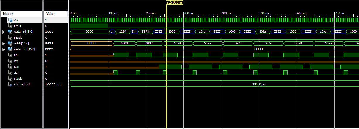
5678 JMP >567A   * effectively a NOP
567A JMP >5678   * branch back to previous line
![]()
TMS9900 compatible CPU core in VHDL
Retro challenge 2017/04 project to create a TMS9900 compatible CPU core. Again in a month... Failure could be an option...
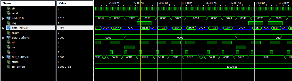 The core does a few extra memory accesses (it reads register 0 needlessly twice) so the execution takes a whopping 6 memory reads and one memory write (IAQ signal marks opcode fetch - from yellow line onwards). Thus, despite the 100MHz clock, this instruction takes almost 500ns. I will remove the unnecessary R0 reads (that's an instruction decode artifact) later. For now I am just happy this works!