 Dr. Cockroach
-
1Step 1
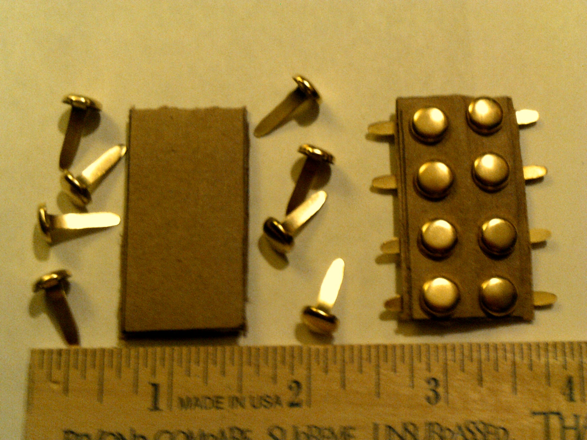
The Cardboard Logic Pad - The basic logic building block for the construction of IO
-
2Step 2
![]()
This is the start of building a Cardboard Logic Pad or CLP for short. The cardboard is found as scrap and the paper fasteners are from any local office supply or big box store. These fasteners take solder very well.
-
3Step 3
![]()
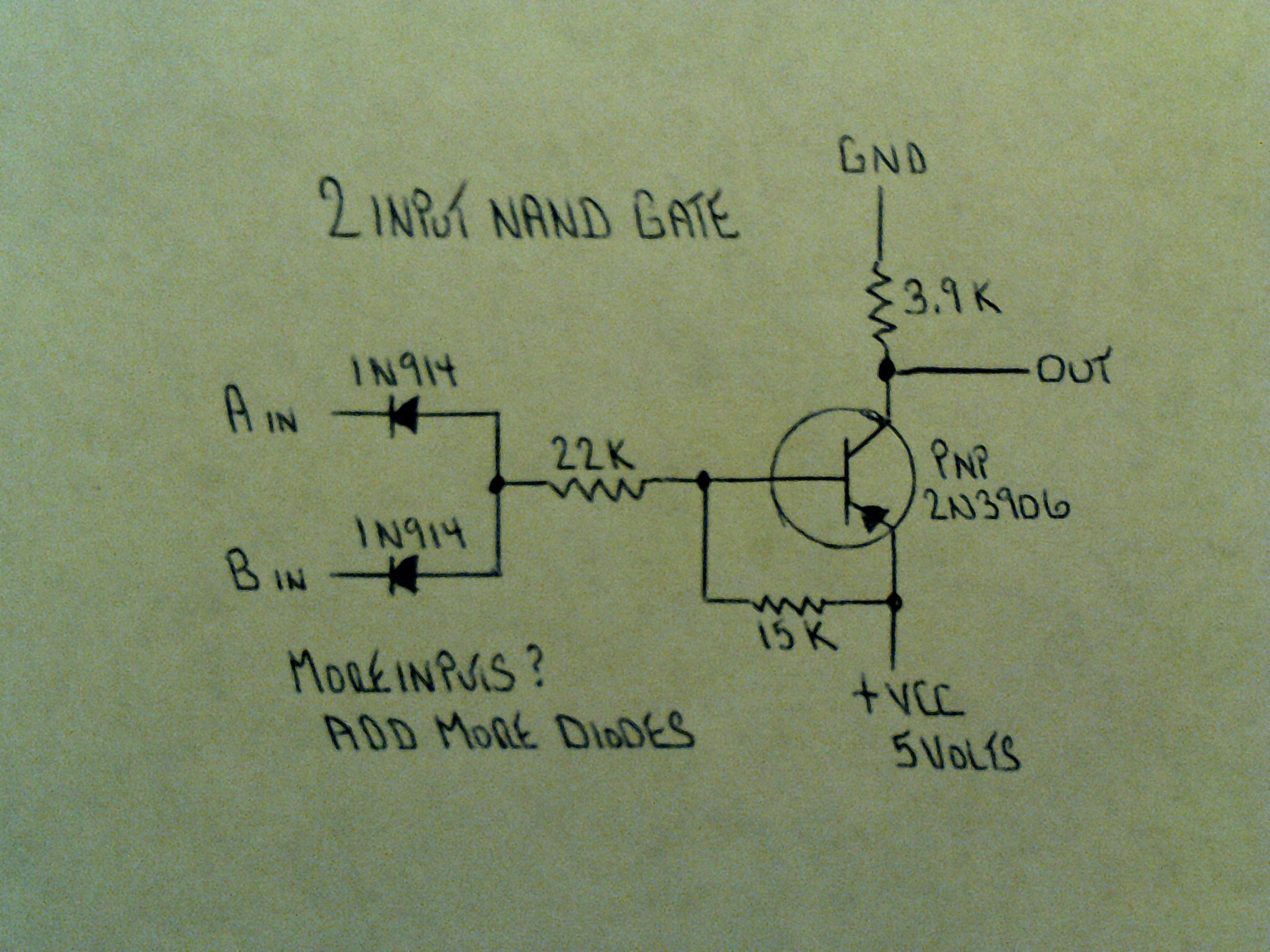
Select the gate circuit that is desired. In this case I am using my basic Nand gate circuit using a npn transistor and input diodes.
-
4Step 4
![]()
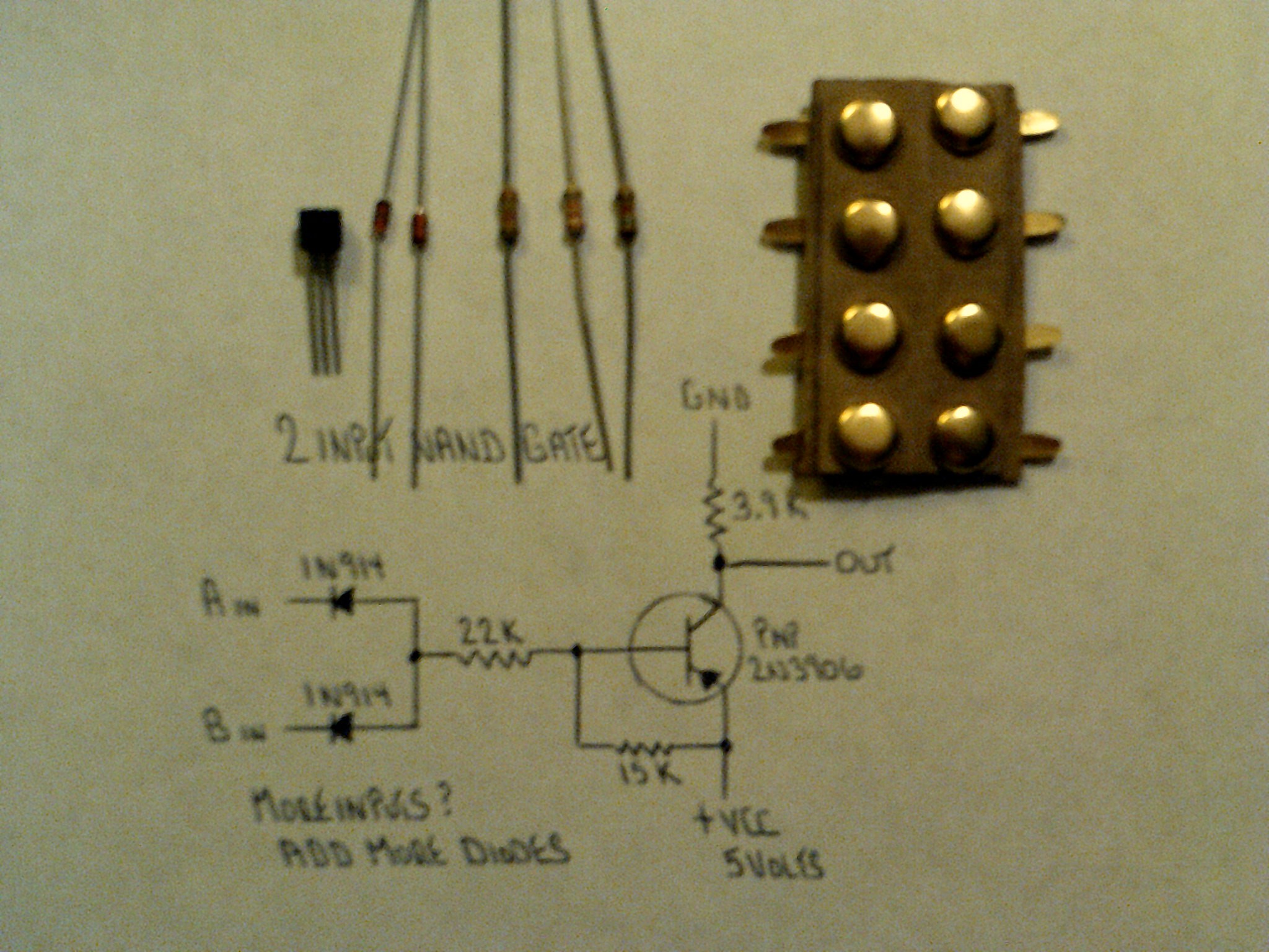
Not that many parts to a gate is there.
-
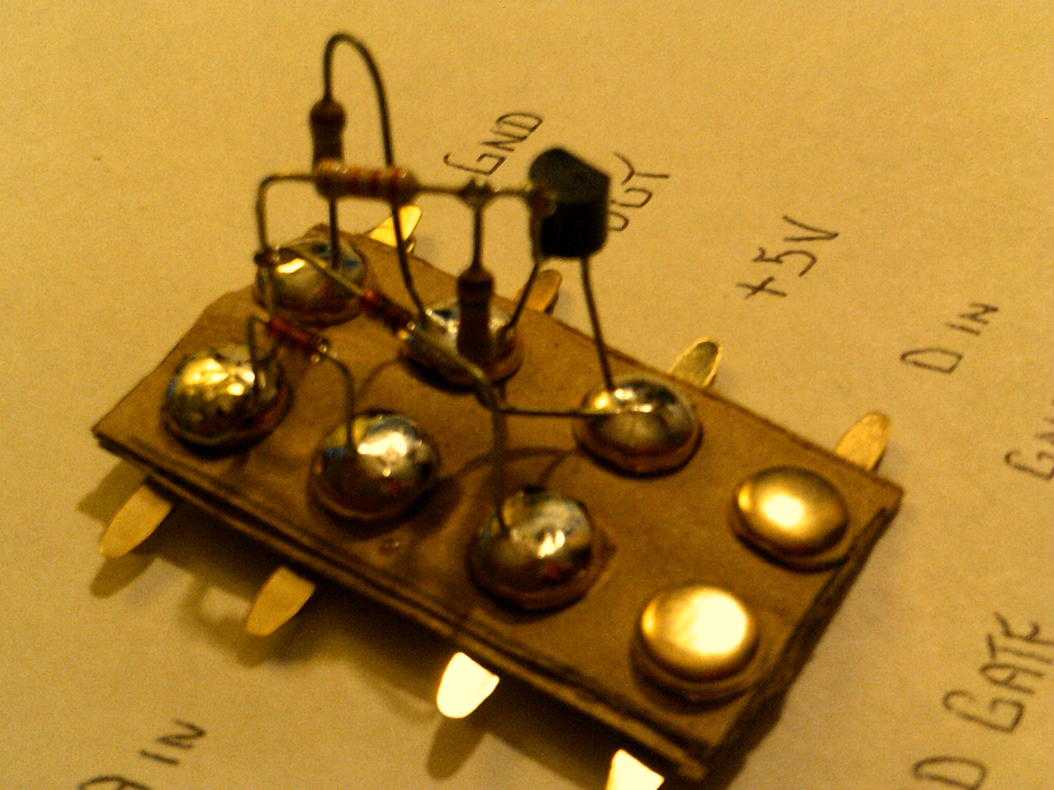
5Step 5
![]()
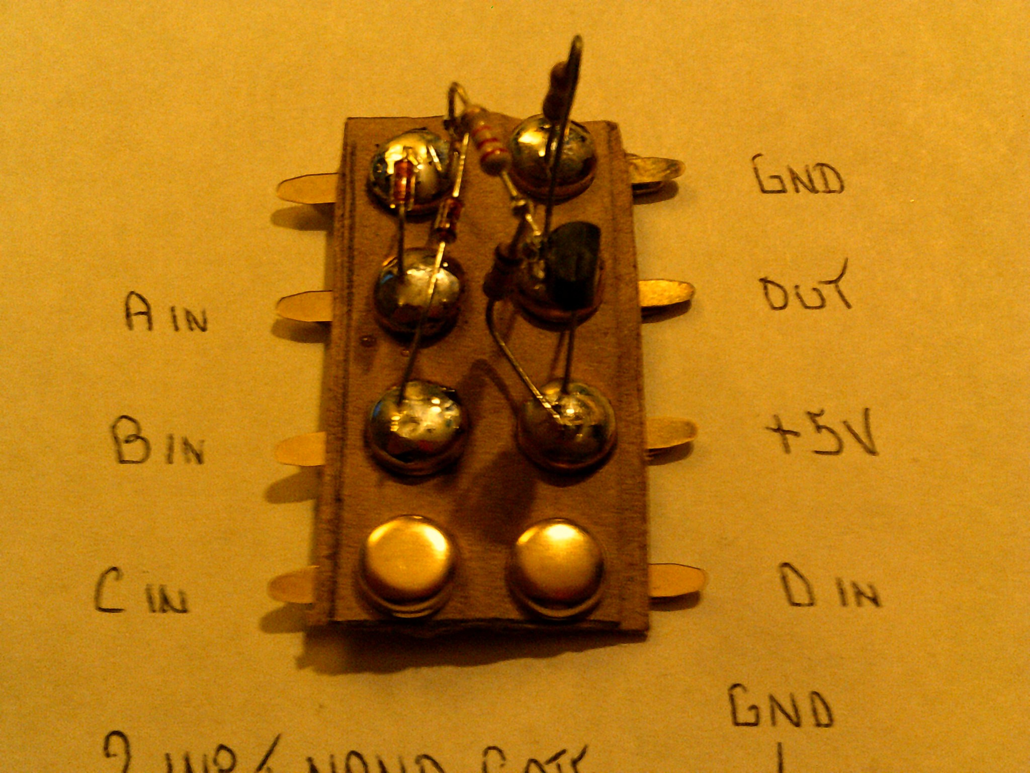
Just as in a IC, the connections on the CLP are kept standard for ease in wiring and trouble shooting. Due to the amount of solder used, A clip should be attached to the transistor leads as a heat sink when soldering.
-
6Step 6
![]()
A very small work of art and yet can be combined with many more pads to create any logic circuit that you want.
IO - The Inside Out Cardboard Computer - bis
My goal is a 4-bit CPU using recycled cardboard substrate and Diode Transistor Logic. This will develop into an educational platform.
Discussions
Become a Hackaday.io Member
Create an account to leave a comment. Already have an account? Log In.
Real cool! What is a measurement of the individual cardboard logic pad?
Are you sure? yes | no
Thanks, If I recall the pad measures about 1 X 2 inches and was chosen due to the metal fasteners used. Not the best use for space but great for using home materials and easy to modify :-)
Are you sure? yes | no