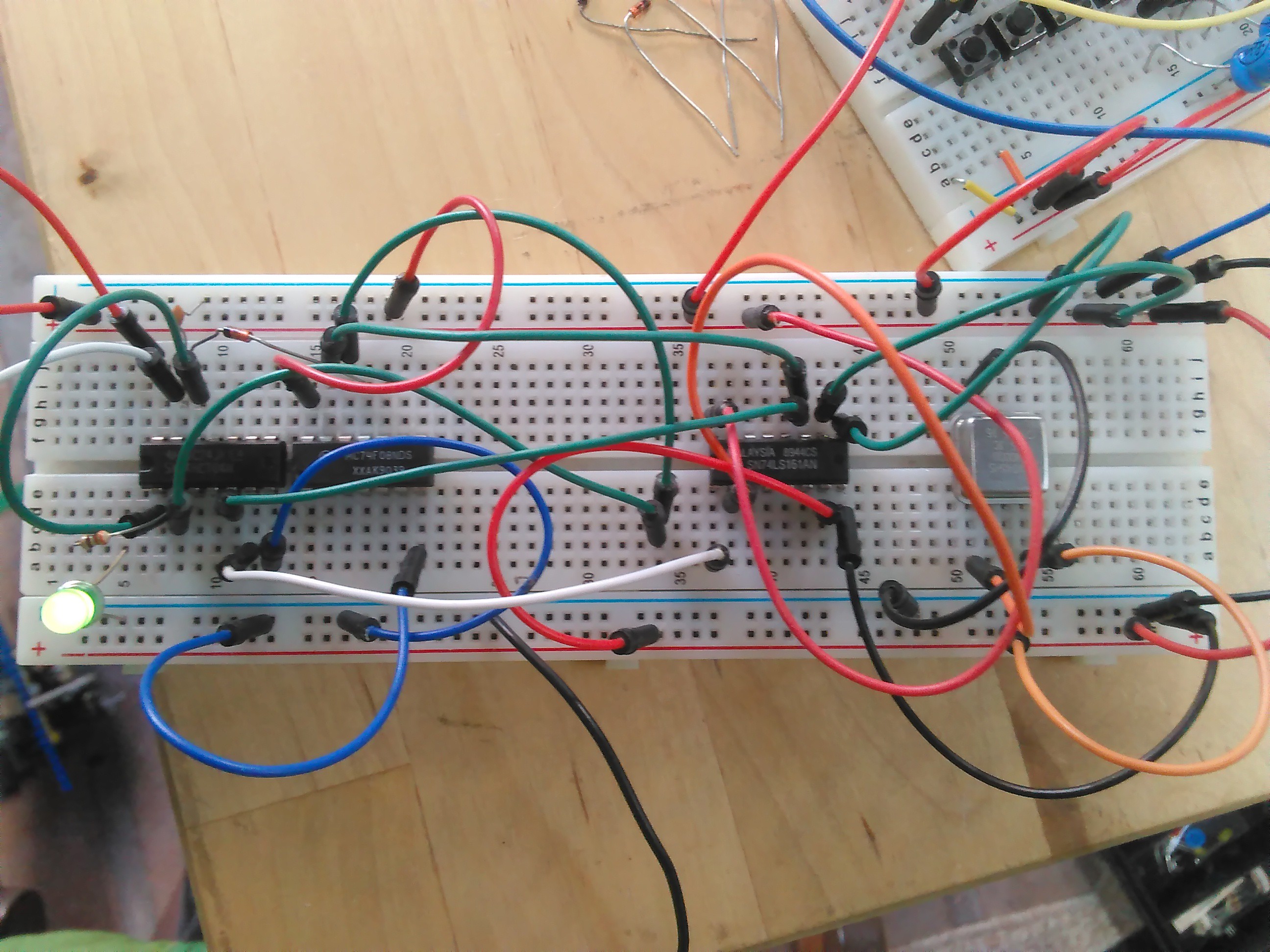
My current working design uses a buffer gate for each bit of data. A capacitor connects to the input of the buffer. A diode goes from the output of an AND gate to the capacitor, positive lead to the AND. The AND's inputs connect to the output of the bit's buffer gate and to the refresh clock. For the buffer I used 2 NOT gates, which works well. Im going to create an array of maybe 4 bytes for test. Here is an image of what I have so far:

 Dylan Brophy
Discussions
Become a Hackaday.io Member
Create an account to leave a comment. Already have an account? Log In.
Can't wait for a schematic :-)
It looks similar to what I do with the relay computer, but with TTL :
https://hackaday.io/project/18757-ygrec16-ygs-16bits-relay-electric-computer/log/49877-capacitors-and-diodes
https://hackaday.io/project/20864-ygrec-15-bis/log/56536-dram-again
https://hackaday.io/project/18757-ygrec16-ygs-16bits-relay-electric-computer/log/50480-dual-diodes-the-hard-way
https://hackaday.io/project/18757-ygrec16-ygs-16bits-relay-electric-computer/log/56214-new-dram-array (read this !)
Are you sure? yes | no
Thankyou for those recources! I will look into them. I need some better design ideas anyways so this is awesome.
Are you sure? yes | no
that's just the motivation I needed to start prototyping my first 16×16 DRAM array :-D
Are you sure? yes | no