 Jan Petrik
Still Fixing the stuff I missed on last revisions.
One of the more shameful mistakes was thermal design of main 5V buck. It could not deliver 3A with temperatures I would consider reasonable.
I kinda did not pay enough attention to small print in the datasheet |O. Go and take look at PCB that is used for specifying package thermal resistance, that PCB is bigger than you would expect...
I sandwiched buck be
tween edge of pcb and RPI connector. I missed my goal of 3A output by about half an amp. Also I did not verified used inductor beforehand, AC losses were way to high. So for next revision I've improved thermal design for buck and diode. Since I have a little more board estate I can go for a bigger inductor. Samples are on the way(WE 74437358047). And I'll test the inductor before sending boards to production.
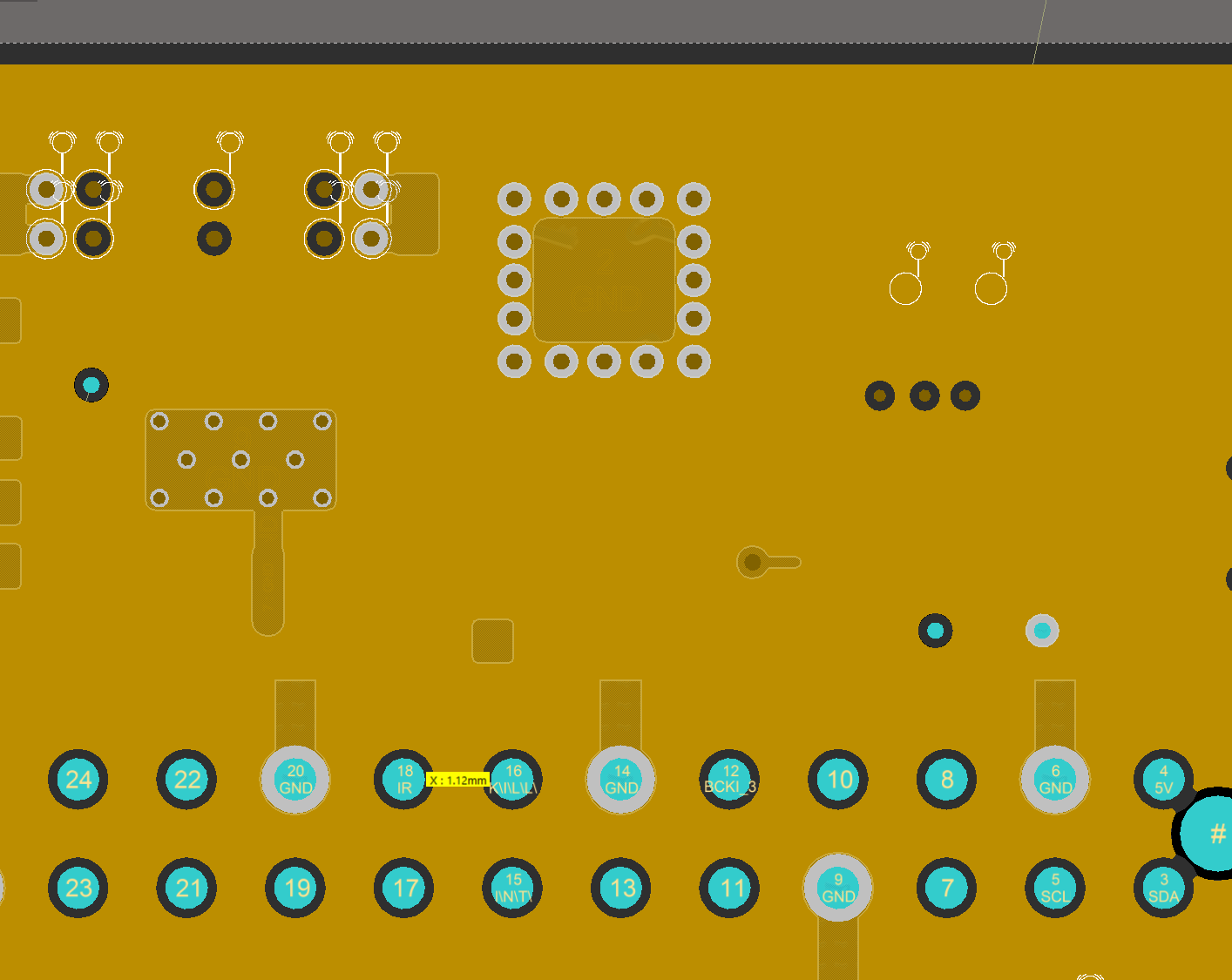
I've also discovered that I did not performed "remove unused pad shapes", so there was not really much copper in the ground plane in between RPI connector. That compromised heat transfer into the rest of the board. That is fixed now, so hopefully we'll get better cooling. I'll probably go for 35um copper thickness on next PCB as well - to see the effect of changes. As you can see the difference in web width is quite big - actually now its more than twice the original width....
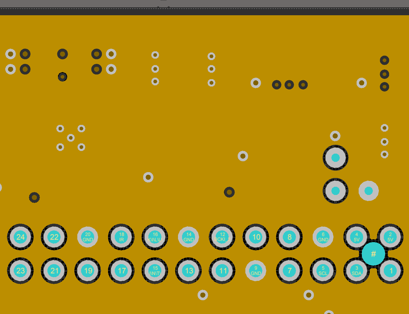
Old:
New:
Discussions
Become a Hackaday.io Member
Create an account to leave a comment. Already have an account? Log In.