Close
0%
0%

Nokia 3210 Retro Fit Board

Mainboard that retro fits a Nokia 3210 mobile phone.

Similar projects worth following
The classic and nearly indestructible Nokia 3210 mobile phone was state of the art. Nowadays it can merely bring a smirk on your face when you remember the old days of snake on the dual color lcd screen. This is about to change.

I am going to build a board, that fits into the space where the circuitboard of the old Nokia 3210 sits. It will come with the same layout for buttons and LEDs. The screen will be replaced by a OLED display that is much more beautiful than the original dual color TFT display.

For the CPU the current design is build around the STM32F756 but I am not sure if I want to stay with the part. STM is currently building a much more capable processor. The STM32H753 with lots more RAM, Flash and MHz. It packs 2MBytes Flash, 1MB RAM, 400 MHz CPU and lots of peripherals into the 100 pin LQFP on the board and it is Pin compatible to the current MCU.

The current design comes with an ESP8266 Module but that does not provide Bluetooth. This needs to be revised.

  • 1 × STM32F756VGTx Microcontroller 1 MB Flash, 320+16+4 kB RAM, 216 MHz
  • 1 × 160x128 OLED Display SEPS525
  • 1 × A7 GSM/GPRS Mobile Radio Module
  • 1 × ESP8266 WiFi Module

  • Moving slowly but moving

    Platinenmacher11/19/2017 at 11:38 1 comment

    So I finally got the boards made. 6 layer boards are hard to get made for a reasonable price. I got 10 boards made by EasyEDA for around 180$. Compared to others it was quite cheap. The boards took 4 weeks to produce and came in the mail without issues.

    I did not get a stencil made. What is something i kind of regret now. On to soldering the components by hand...

  • Let's go shopping

    Platinenmacher09/14/2017 at 20:51 0 comments

    I shopped around to get some of the parts for the phone. Doing so I found some awesome crystals for the MCU. So I am going to change the footprint for those.

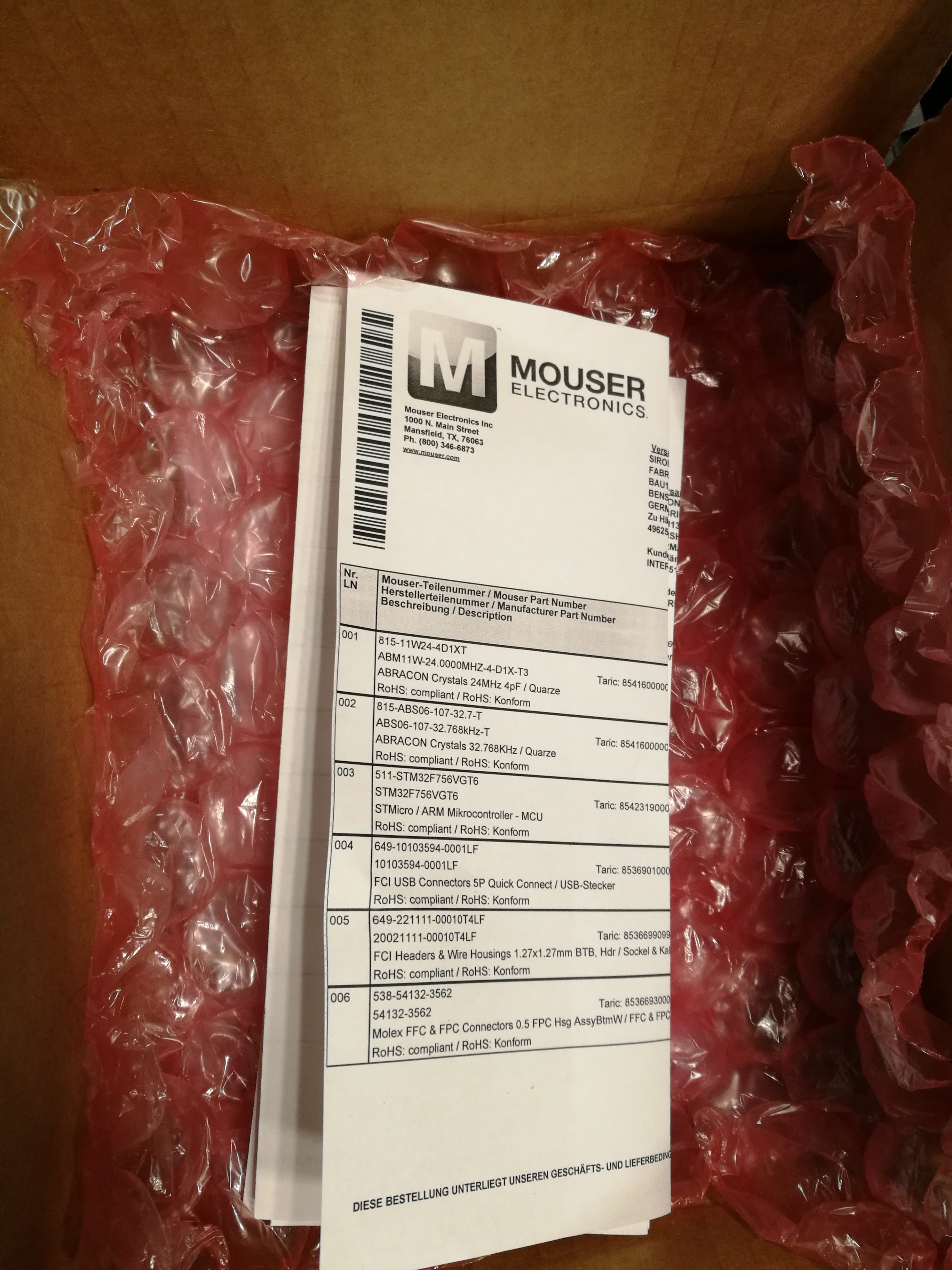
    The first package arrived today. Crystals, MCU, USB Connector, JTAG Connector and Display Connector. 

    During the weekend I can finalize the design and get some boards made.

  • Prototype PCB done. There comes the review.

    Platinenmacher09/10/2017 at 19:34 4 comments

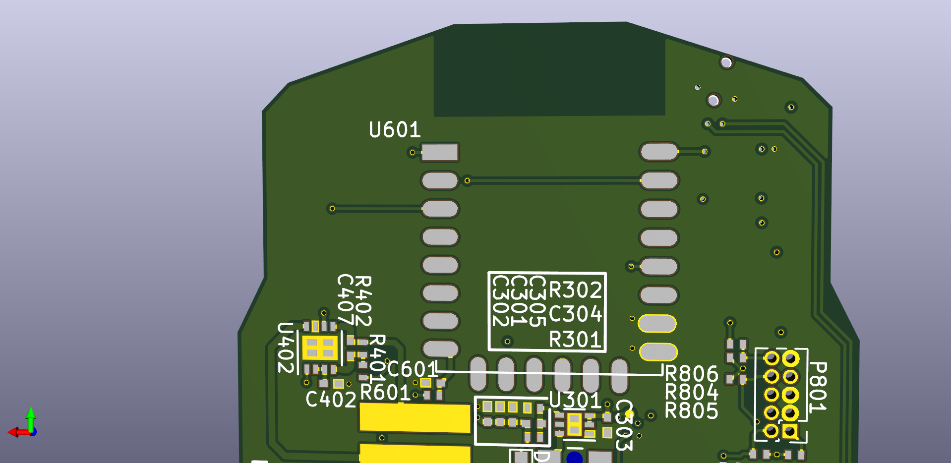
    Over he weekend I finished laying out the PCB for the phone. It was quite challenging to route all the signals on a rather small board. I decided to go for 

    • 6 Layers (Signal, Power, Signal, Signal, Ground, Signal)
    • 0.2mm track width
    • only through hole vias 0.5mm copper / 0.3mm via drill size (some are 0.45mm copper)

    That should come to approximately 25€ for a fabricated PCB. So that is acceptable.

    There were some tricks necessary though. Here are some 'interesting' parts of the design:

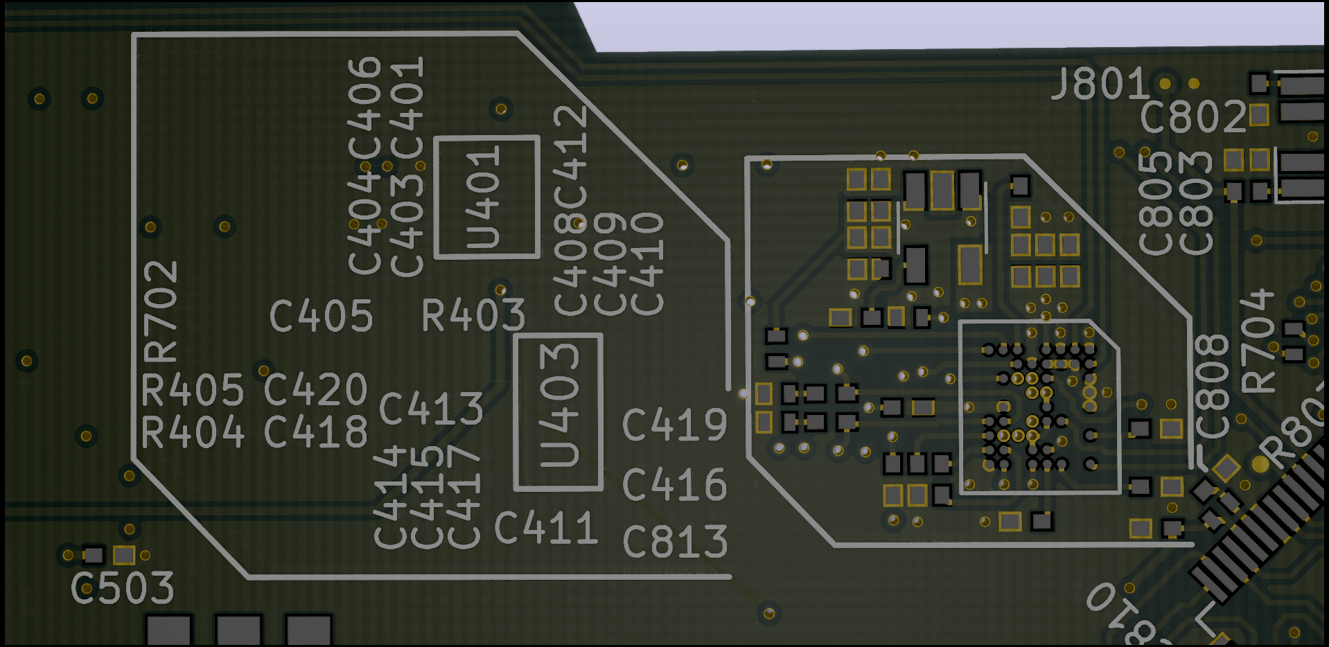
    This shows the finished part of the Audio Codec I picked for the i.MX7 project. It does come in a small BGA package ant therefore doesn't need a lot of space. If you work on an HDI board this is no problem. You can probably route a 0.1mm trace through the balls and use micro vias in pad to go to lower layers. Not so for this board. We only have through hole vias. So as we do not need all the balls of the grid we can ignore them, right? Right? OK lets void those pads. There you have it. Enough space to fan out all the remaining signals. We are good to go. Let'S see if this actually does work. Would be a nice hack.

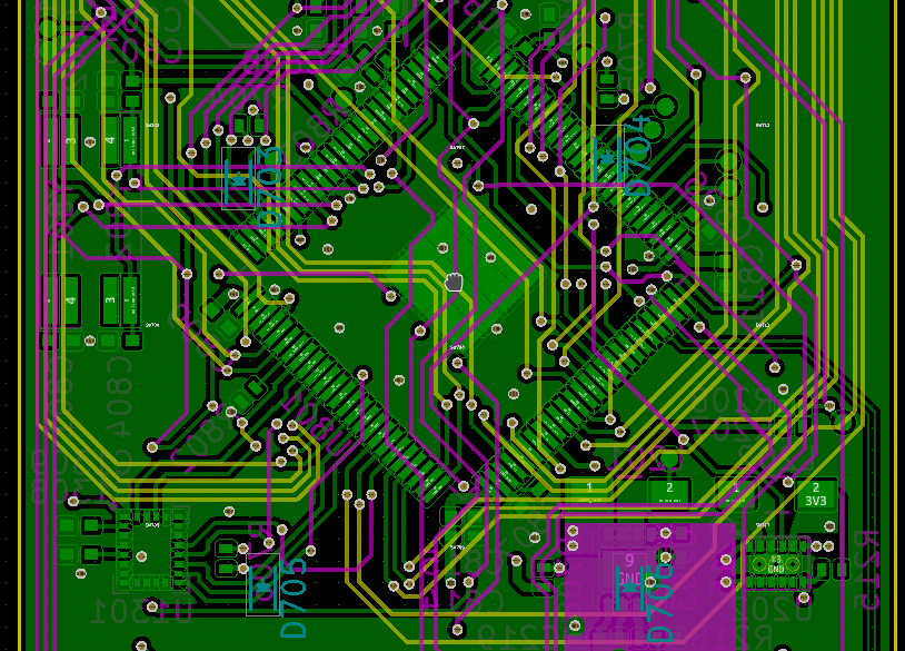
    The CPU takes a lot of space on the back side of the board. Compared with the big button pads on the front we have not that much space left for vias. This fanout is very convoluted and is probably way to complicated. But it is connected and should work.

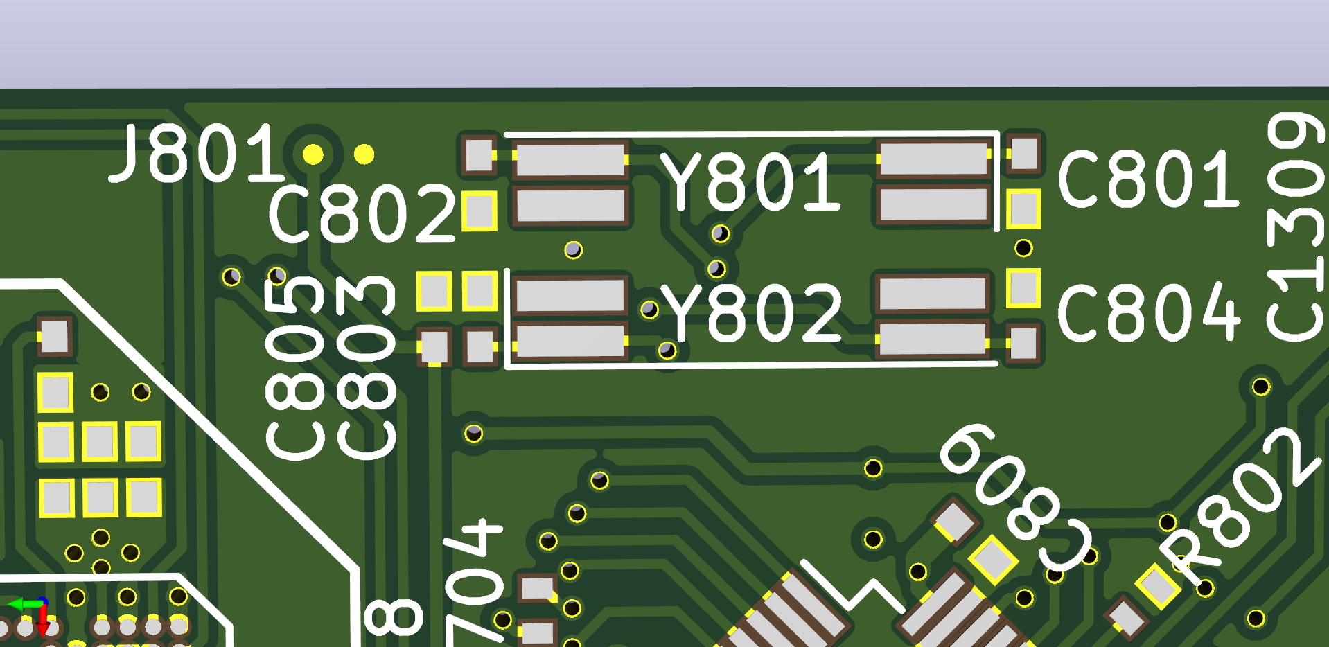
    We have two crystals here. One 24MHz for the CPU (goes to 216MHz internally) And another one for 32kHz real time clock. Combined with the GPS signal from the A7 radio module we should always have an accurate time. Nice.

    Up here we have the infamous ESP8266 radio module connected to the CPU with UART signals. So we have GPRS and WIFI network connection available.

    Now I let the design sit for a few days. Later on I will have a second look at the whole circuit and layout to find some errors before I order the first batch of boards.

  • Small changes big issue

    Platinenmacher08/30/2017 at 14:51 0 comments

    Over the last weeks I familiarized myself with the KiCad source code. It is a huge project with several programs that use a common code base and extend it to fulfill all the needs for electronic design. But does it?

    I found out that KiCad limits itself. The micro vias placement is restricted to outer layers only. But with this design I am going deep into what is call HDI technology; High Density Interconnect. I have a regular 4 layer PCB which has two additional layers attached to it. 

    With the patched I submitted you can turn KiCad into a 'I know what I am doing' mode. Which meas you can place any type of via anywhere. You should not do it though. Vias are pretty well constraint by the manufacturer of the board. Since KiCad does not know of any layer thickness, production technologies and such it restricts to what is a sensible lowest common denominator.

    For anyone interested to have a look at my work: look here

    Routing of the DDR3 part is still on my todo list though.

  • Constraint Routing in KiCad

    Platinenmacher08/05/2017 at 11:05 0 comments

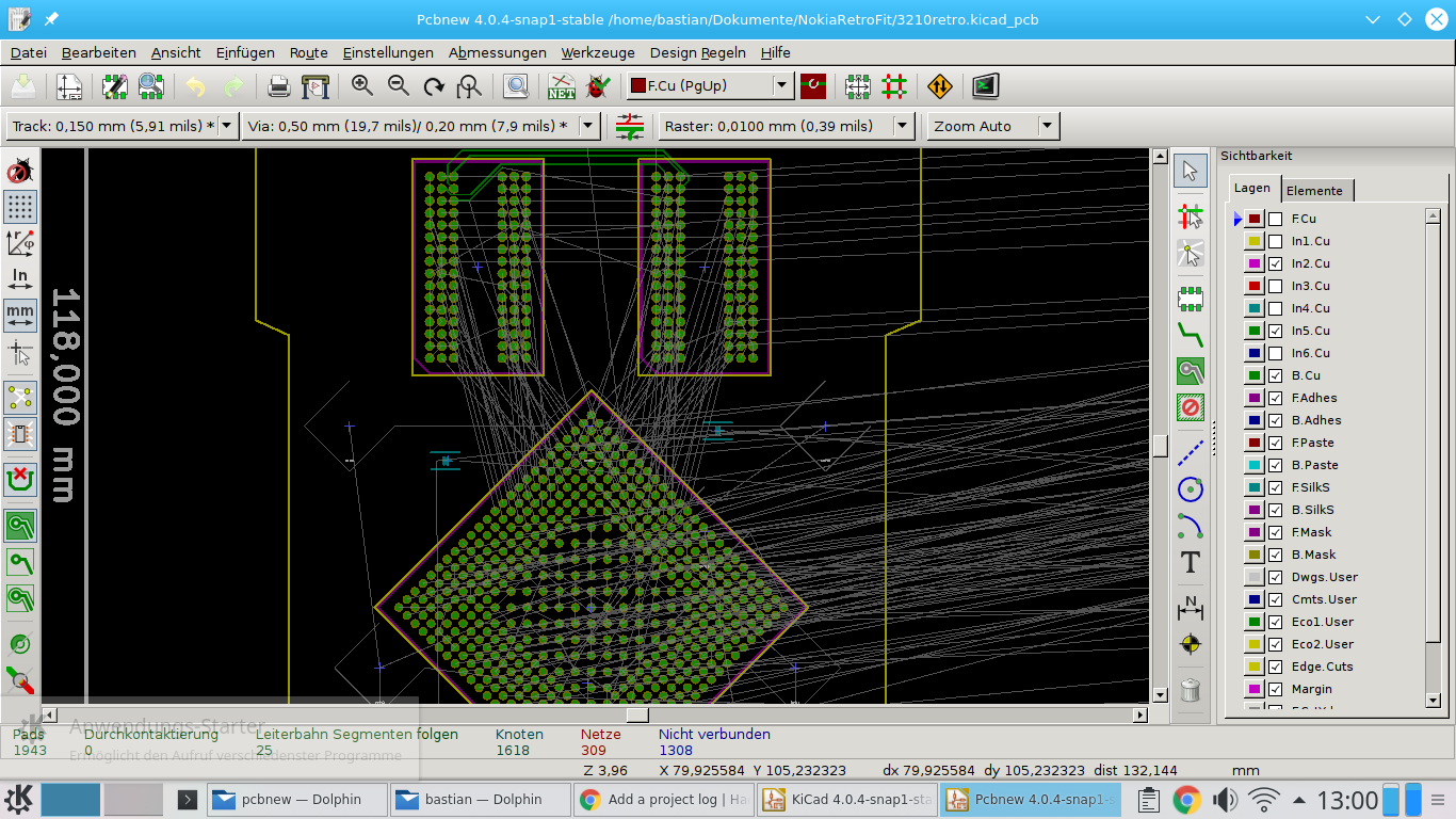
    I am at the point where I need to route the DDR3 Signals of the CPU core. What that means is that I have a bunch of signals that need to be routed to the same length to two different chips on the board. I think the rats nest tells a lot about the thinks to undertake for DDR3 routing. 

    KiCad is very limited in the features making the job a little easier. So my next endeavor is to put some features into the KiCad source-code to give an overview of the track length and stuff like that. 

    If you can read German you can have a look at my Blog for some detailed information.

  • Let this be clear. This is ridiculous

    Platinenmacher06/25/2017 at 17:57 0 comments

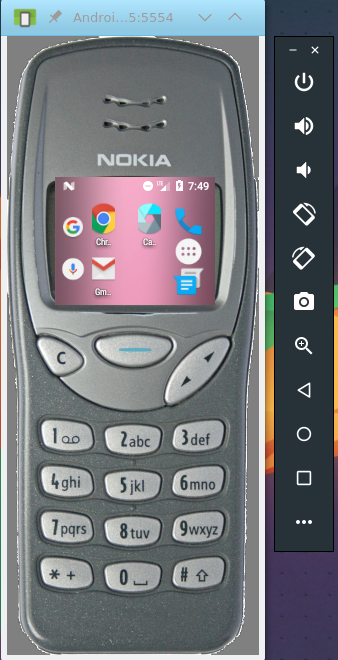
    Ok I know that this project sounds ridiculous and it is. Android is not meant to be put into a stamp sized display. But lets be honest: It would be really cool to have a working old Phone with modern technology. So I am still going to do it. As a little taste here is how it would look like if you just start up Android on a screen that 'big':Not really usable to be honest but I am trying to build a menu that can give you all the phone functionality I want. Or maybe I stick to Linux and build a GUI for it. But where is the fun in that?

  • Schematic Overview

    Platinenmacher06/16/2017 at 09:41 0 comments

    OK let's try this video thing. This is the first time I did a video like this so be gentle :)

  • eMMC and the horrors of Datasheets

    Platinenmacher06/15/2017 at 10:25 0 comments

    I wanted to add an eMMC (16GB) mass storage to the Mainboard. But currently I am unable to find any documentation about the chips from the big vendors. I tried Micron and bounced at the form to get an NDA. I tried Toshiba and did not get any information at all. I can buy them from mouser for sure, but no datasheet what so ever.

    This is very upsetting. But I am going on to try and find a suitable eMMC. I do not want to stick to SD card for the main operating system since they have the tendency to die after a while of usage. They also only have 4 bit compared to the 8 bit data bus of eMMC.

  • Things Coming Together

    Platinenmacher06/11/2017 at 16:24 0 comments

    After I split the repositories into sub modules I started shuffling things around in the schematics. There is not very much done, but the switch to i.MX7 CPU is coming along. I copied the PMIC and DDR design from my test project and merged it into the current design. Next big thing will be mass storage and multimedia. I want to keep up the current design where I can switch between mic as input for the GSM module on the one hand and CPU as source on the other.

    I played around a little bit with the Android build system. It is big. I think I need to go a little bit deeper into it to finally wrap my head around it. Anyone there who has experience with building Android?

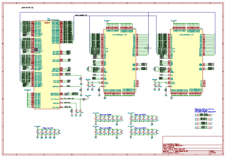
    This is the RAM schematic so far. Data signals will be assigned when it is tie to route the bus to the chips.

  • Cleaning up the Github Repository

    Platinenmacher06/06/2017 at 05:34 0 comments

    I see that the Github repository for the project is getting a bit convoluted. As with any other project there are parts that can be used in other stuff as well. So I want to split up the data into a couple different repos.

    The footprints shall go to a footprint repo. As should the schematic library. Software should be completly separated from the board data. Documentation and Information should be kept with the board data.

    Therefore I want to have is sorted like this:

    Board Repo:

    • KiCad Project
    • Datasheets
    • Documentation of circuit
    • Link to KiCad schematic repo
    • Link to KiCad Footprint repo
    • Link to Software repo Android
    • Link to Software repo Applications

    Now let's find out how to do this.

View all 12 project logs

Enjoy this project?

Share

Discussions

Lukas wrote 09/14/2017 at 15:17 point

This is awesome project.I would really love to have phone like this.If you make it work will you make kickstarter or will you sell this?

  Are you sure? yes | no

deʃhipu wrote 06/15/2017 at 16:38 point

This is a great idea! Where did you find the oled display?

  Are you sure? yes | no

Platinenmacher wrote 06/15/2017 at 19:11 point

I discovered it by accident. I was buying smallish OLED displays from Aliexpress for something else. Turns out it fits exactly in the diplay frame of the 3210.

  Are you sure? yes | no

deʃhipu wrote 06/15/2017 at 19:22 point

Do you have a model name that I could look for?

  Are you sure? yes | no

deʃhipu wrote 06/15/2017 at 19:29 point

Nevermind, found it, SEPS525, thanks!

  Are you sure? yes | no

Does this project spark your interest?

Become a member to follow this project and never miss any updates