Now that I've accomplished a milestone for the software (the BM9 benchmarking), I'm thinking I should swing back to developing the TTL version of the system. I'm pretty happy with the architecture. So I've been going back and doing the implementation in TTL. Eventually I'll make a PCB with it, but I might prototype it on a breadboard first.
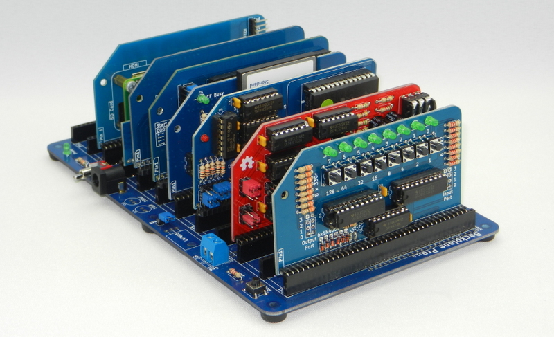
I'd like to split the project into two separate boards: an S100-inspired backplane with the CPU in one slot, and the peripherals in another slot. Here's an example I found on Google search for illustration:

Maybe I would have a separate clock board in another slot, but I may integrate that with the CPU. Maybe I would have a debug board which shows the data/address bus with LEDs. Of course having a big backplane would be expensive, so I'll have to see how large these boards need to be. And if I have all my boards stacked up, then they don't show off all their components as well. Looks go a long way. Perhaps I'll just split it into two just to illustrate how one board is the CPU, and the other side is flexible with ROM/RAM/UART, etc. Then I can lay them side-by-side and still be able to show off all the chips.
But schematic comes first, and I'm only maybe 1/3 of the way there.
image source: http://rc2014.co.uk/
Discussions
Become a Hackaday.io Member
Create an account to leave a comment. Already have an account? Log In.