Recently I found a board maker similar to OSHPark, but based in Germany, Europe. Could it be that my wish came true? As soon as I had a new version of PewPew's PCBs designed, I decided to try them.
The prices seem similar to what OSHPark offers: at OSHPark I paid $8.95 for three 2.00x0.90 inch PCBs, here it's €8.43. However, OSHPark has free shipping (which constitutes the bulk of the waiting time for me), while Aisler charged me additional €4.96 for shipping. But that's totally fine by my if the boards land in my mailbox faster this way.
There is a bit of disappointment here, though. I made my order on 28th of September, and for nearly two weeks nothing happened. I finally went to check the order's status two days ago, and it said on the website that they will be fabricating it within 1 hour. I assumed that it's just a fancy message, but indeed one hour later the message changed to information that they are shipping it within minutes, and later that day that it shipped. The boards arrived two days later.
So in theory, it could be much faster than OSHPark, which usually makes my boards within a few days, and then they take two weeks to get here. However, in practice waiting for fabrication made it about the same. Perhaps it will get better as they get more orders and the panels will fill up faster?
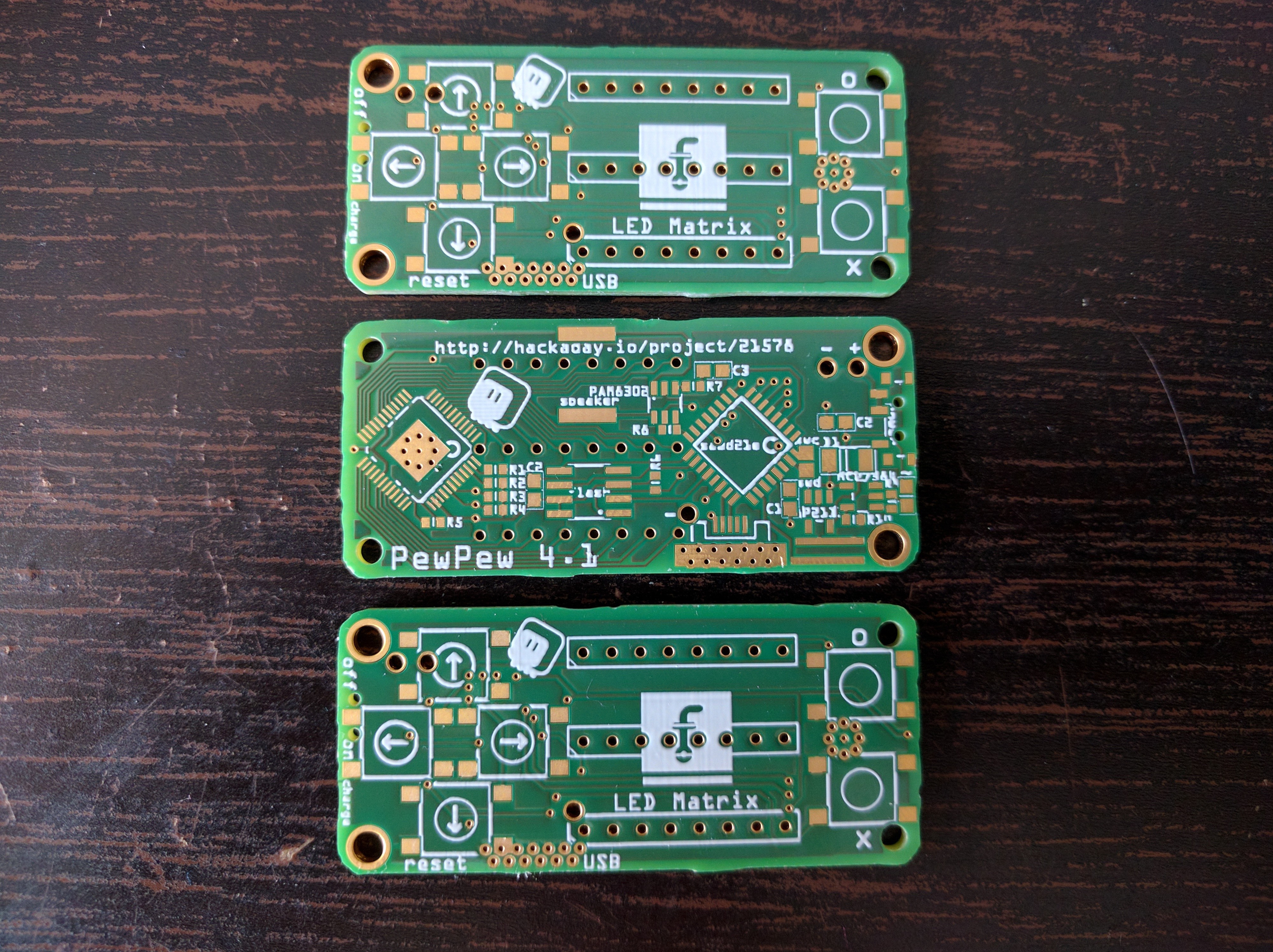
Now about the boards themselves. Here's a photo:

First of all, as you can see, the boards are green. As with OSHPark there are no color options, which is fine, but green is a bit boring. Their website is all orange, it would be super-awesome to get some orange boards! Oh well, green is fine.
There is ENIG finish, just like with the OSHPark boards.
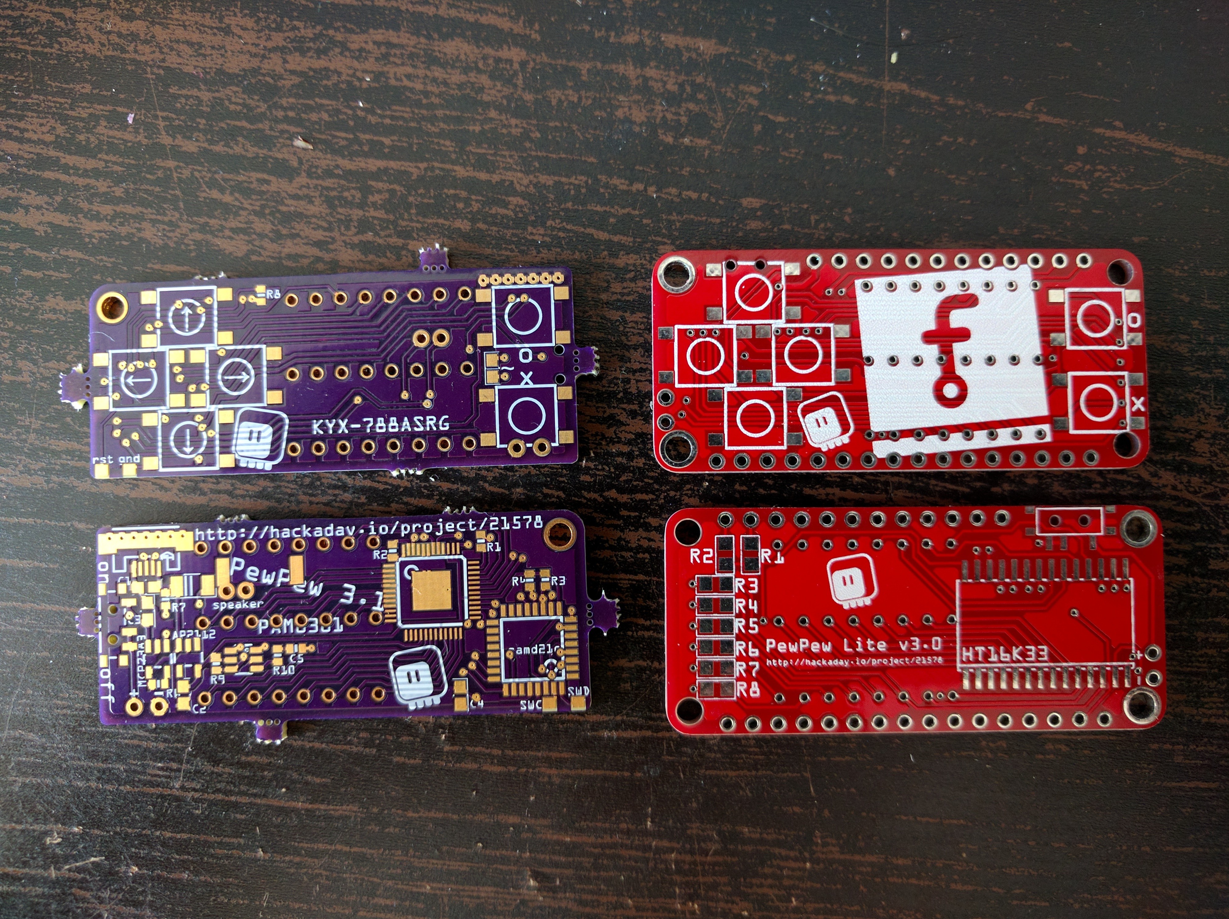
Both the solder mask and the silkscreen are much lower resolution than what you get with OSHPark. If you look at the chip footprint on the left, you will see that every pin pad is different width — that's the effect of low-res solder mask. You can also see that the head of the sheep logo bled into the outline — that's the effect of low-res silkscreen. For comparison, boards from OSHPark and SeeedStudio:

Finally, the board outline. I'm really shocked about that: it looks like it was cut out with a hatchet by a drunk worker. I guess I shouldn't have ordered during the Octoberfest.
I still need to assemble the board and see if it works, but all the traces look fine visually. We will see how that goes.
 deʃhipu
Discussions
Become a Hackaday.io Member
Create an account to leave a comment. Already have an account? Log In.
Hi Radomir,
Felix from AISLER here. First of all thank you for this review and your very honest feedback. I would like to give you a bit of insight into why things turned out that way.
Regarding the milling of the outline, indeed this must've been an Octoberfest mishap, I must admit. Since we don't like tabs/bridges at the outlines of the PCB, we decided that the final manufacturing step is a milling to get rid of them. We've had some issues with that in the past and you must've been got in a run where it wasn't solved yet. I'm sorry you were caught in this crossfire.
Silkscreen is a problem we've been discussing with our manufacturer. Especially with Fritzing Fonts they tend to have a few problems because they use Inkjet, which is usually much more suitable for series manufacturing (where silkscreen doesn't matter that much). This, however, is something we can't solve quicker, so we are thinking about some workarounds. However, we are unfortunately not talking about quickwins here.
Regarding the time this was actually not Octoberfest related but there was a German public holiday (German reunification). While this is a great day for German democracy, it didn't help our delivery times. So, we usually ship within 7 business days.
Looking at the solderresist, it should actually be very precise. So if you zoom in, every pad on the IC should have a bit of solder-resist left. The indicator that it is correct is a halo of yellowish/brown stuff at the golden pads of the footprint. When you look at the footprint on the right of the purple board you will notice that there is no halo but that it's completely yellowish/brown, which means that the solder-resist has been taken away completely. Fabs like to do that to save time so that the individual pads do not need to be modified (the red board did the solder-resist fine by the way). However, we forbid our fabs to take that shortcut. It's possible however that the change is also in your IC's footprint and since you showed different versions I would be happy to see the original data to see what you have manufactured.
By the way: Our boards all come electrically tested for functionality, so if we haven't informed you about failed tests, your boards should work as you specified them. We run these tests to insure that there are not bad surprises after mounting the parts on the PCB.
By the way 2: Obviously the board outlines look horrible, it devalues the whole circuit board, which is very unfortunate. In that case, we usually offer our users to remanufacture the circuit boards if they are not happy. For that users can reply to any of our emails directly.
I’m looking forward to hearing your feedback.
Cheers
Felix
PS.: We usually send out e-mails on every manufacturing step, so you should have been informed about the ordering process. Was that not the case?
Are you sure? yes | no
Thank you for your reply. I guess I was pretty unlucky with this. Just to make this clear — those are prototypes, and I don't mind the rough edge or low-res silkscreen on them. I was just comparing it with the boards I had manufactured earlier.
Interesting point about the removed solder mask on the purple PCB — I never noticed that myself, interesting. I would probably also not notice the differences in widths of pads on your board, if the silkscreen didn't catch my attention. In any case, both of my uploaded gerbers are the same with respect to that particular footprint. Here's a close-up from gerbv of the solder mask:
And of the copper layer:
You can see that in particular, pads 13-15 are pretty much the same. Now, looking at the fabricated PCB:
You can see that pad 15 is clearly narrower than pads 13 and 14. Also pad 17 has a border around it, and pad 19 is again much thinner than the others.
My comment about testing if the PCB works was referring more to my own mistakes in the design, rather than to problems with fabrication — sorry if it sounded otherwise.
Yes, I got e-mails, but somehow I only saw them after I already checked the website.
In any case, I'm very glad that you take this seriously, and I'm really looking forward to being able to fabricate the boards in Europe at such convenient terms. I'm sure you will work out any problems you have right now.
Are you sure? yes | no
By the way, I just found a horrible mistake thanks to looking at those gerbers — one of the traces on the bottom is way too close to a pad. Fortunately that pad is not connected to anything, but it doesn't make me feel good that I missed it.
Are you sure? yes | no
Hi Radomir,
we allowed ourselves to remanufacture the boards. We will send them your way today along with a Stellar Stencil for your convenience. And again, sorry for the little hickups.
If there is anything, please do not hesitate to contact me directly.
Cheers
Felix
Are you sure? yes | no
Thank you Felix. This is an old version, and I have moved with my designs further already, but it will be very interesting to compare the quality. I feel bad for giving you a bad review, but I'm trying to be honest. I will write another review once the boards arrive.
Are you sure? yes | no
ouch, that board cutout is rough. but i do hope you (and Dave) find a worthwhile domestic option, nothing kills project motivation like shipping time.
Are you sure? yes | no
I actually think that this long waiting time gives my project a certain rhythm, giving me time to think, a little bit like the "slow web" (https://jackcheng.com/the-slow-web). I've actually noticed that PewPew has recently become more like work than hobby, and that would explain why I'm looking for faster options. As long as it's only hobby, I don't much care about speed — I will get there sooner or later.
Are you sure? yes | no
I have to do the same comparison with my #LAMEBOY - another ESP12 handheld - I got the boards between Zurich and my trip to America and "owe" them a comparison between boards. My outlines looked way better, iirc. I should order smaller boards incognito and compare them.
Are you sure? yes | no